In this day, given the availability of SIMM modules it would be tempting to concentrate only on these parts. But, to do so would bypass a large supply of surplus parts that might be very attractive to homebuilders. We will then examine several different types of DRAM chips. The main distinction between these parts is whether they have bi-directional I/O pins, or separate IN and OUT pins. Another distinction will affect refresh. Will the device support CAS-before-RAS refresh, or not?
Let's begin at the beginning. Let's have a look at some basic DRAM timing, and how we might implement it.
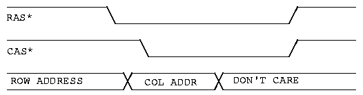
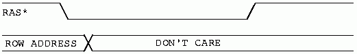
The basic timing diagram for a read cycle is shown in figure 1 above. Two control signals are used to sequence the address into the device; RAS, or Row Address Strobe, and CAS, or Column Address Strobe.
The address is multiplexed into dynamic memories to conserve package pins. To access a 64K DRAM device, you would need sixteen address lines. Without multiplexing, this would require sixteen pins on the package. That's a lot of pins. By today's standards, a 64K DRAM is very small. To support a modern 16MB part you would need 24 pins. This would lead to some very large device packages, and reduce the number of them that you could place on a single PCB.
Multiplexing the addresses saves package pins, and allows the device to fit into a much smaller package, at the expense of a more complex circuit required to operate the devices when compared to static rams. We will discuss a variety of DRAM devices here, but, for now, let's stay with our 64K DRAM. This will be the smallest (in capacity) device we will discuss. It is included here because they are plentiful, and VERY cheap, on the surplus market. This would make them ideal for use in hobbyist projects.
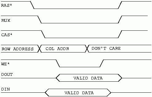
Let us review the timing diagram in figure 1. On the top row of the diagram we see RAS*. This is our Row Address Strobe. Next we see CAS*, the Column Address Strobe. At the bottom we see the address lines that connect to the DRAM chip itself. OK. What is this diagram trying to show us? First we present the row address to the DRAM chip. Some time later, we take RAS* low, or active. We wait a little while, then switch the address presented to the chip. Now we present the column address. After we present the column address, we wait a little while, then take CAS* active; low. Since this is a read cycle, some time after CAS* goes low, the memory will supply output data. Simple huh? Righhhhht! Ok. So how do we do it? What do we need to create this kind of timing? The following illustration will give us some hints.
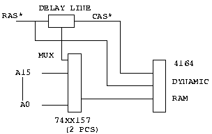
In figure 2 we see the basic dynamic memory controller circuit that has been in use since the late 1970's. No, don't go out and grab your wire-wrap gun just yet. This circuit is not complete. It does, however, illustrate the basic elements needed.
The key element in figure 2 is the delay line. This is a special part that will give precise delays. You feed a signal into the input, then take what you want at various "taps", or outputs. In the past, delay lines were made from 7404 inverter packages. Sections were connected together to eliminate the inversion, and a coil inserted between sections to give the delay. The delay could be controlled by the number of turns of wire in the coils. Today, silicon delay lines are available. Dallas Semiconductor makes a line of silicon delay lines with very precise control of delays. They are pin compatible with the older mechanical ones, and cheaper too.
The first tap is used to generate a signal named MUX. This signal switches the 74xx157 multiplexers to change from ROW address to COLUMN address. The second tap is then used to generate CAS*. This circuit will provide the following timing.
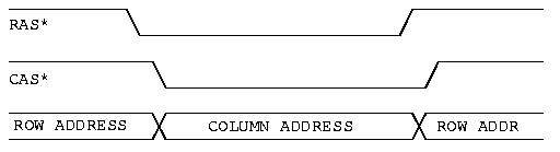
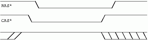
As may be seen in Figure 3, our circuit generates the needed timing fairly well. The astute reader will notice some overlap between CAS and RAS at the end of the cycle. This is not only O.K., but some early DRAMs required it; notably, the 4116, 16k by 1.
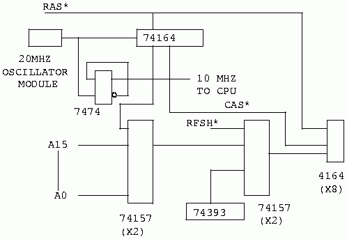
Now let's examine a circuit to replace the delay line. If there is a high speed clock available in the design, we can generate the timing with a shift register. This works best if the CPU clock is also derived from this same source. Let's consider a 10 MHz Z80 design. We will use a 20 MHz oscillator module to derive timing from. The timing generation portion of the circuit in figure 2 could look like this.
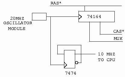
As you can see in figure 4, we start with a 20 MHz clock source. This clock drives a 74164 shift register, and a 7474 D type flip-flop. The flip-flop divides the 20 MHz signal by two, giving us a 10 MHz clock source for the Z80 CPU. The shift register replaces the delay line in figure 2. It is continuously clocked by the 20 MHz clock. RAS* is presented to the data input of the shift register. When RAS* goes low, the shift register begins to shift zeros. On the next rising clock edge MUX will go low. On the following clock edge, CAS* will go low. This circuit will generate the exact same timing as figure 3, assuming a delay line with 50 ns taps in the original circuit. The advantage of this circuit is that it uses cheap parts. The disadvantage is that it requires a high speed clock source. Additionally, the 10 MHz clock source developed in figure 4 may not be acceptable to the Z80 CPU as is (it most certainly is NOT). Additional circuitry may be required to condition the clock before using it to drive the Z80 chip.
The main difference between the circuits in figures 2 and 4 are this. The circuit in figure 2 is ASYNCHRONOUS while the circuit in figure 4 is SYNCHRONOUS. The asynchronous circuit in figure 2 may be easier to adapt to various processors while the synchronous circuit in figure 4 is more predictable when you go to make changes to the design. Consider this. You decide to change the CPU speed from 10 to 12 MHz.
At 10 MHz we are using a 20 MHz oscillator module in figure 4. At 12 MHz, we will use a 24 MHz oscillator. At 20 MHz the period, or time from one rising edge to the next, is 50 ns. At 24 MHz, this is now 42.5ns. Thus the delay from RAS to MUX to CAS is now 42.5 ns. Experience tells me that this is just fine. The only thing we have to worry about now is are the DRAMS we are using fast enough to get data back in time? The fact that the timing compresses automatically when you change the oscillator module will help to speed up the memory cycle; in this case, by 15ns. By speeding up the beginning of the cycle, you have more time for the memory to access. This allows you to run faster with slower memories.
With the circuit in figure 2 you can do the same thing, but you will need
to replace the delay line to get there. This could be a consideration when
upgrading an existing design. Well, if we only ever wanted to read our DRAMs,
we would be about through. However, such is not the case. How does the data
get into the DRAM in the first place? Now I just KNEW you were going to ask
that. OK! Let's look at a write cycle. First we will look at a basic write
cycle. It is not much in use anymore, but does apply to the 4164 device we
are discussing.
In figure 5 we see the timing diagram for a basic write cycle. What is significant in this diagram is that the DRAM device actually does both a READ and a WRITE. At the beginning of the memory cycle we generate RAS, MUX, and CAS, just as we did for a read cycle. Some time after CAS does low, data is available at the output pin of the device.
The interesting thing in figure 5 is that WE gets pulsed low shortly after CAS goes low. Data present at the data input pin is written into the DRAM when WE goes back high. The data presented at the data output pin will continue to be the old data that was in the accessed location before WE was pulsed.
This type of write cycle is referred to as a read-modify-write cycle in some data books. It can be useful in some designs because it will let you use slower memory than you might have needed for an early-write cycle (which will be discussed next). This is because the data is written into the memory late in the cycle; when WE goes high. For early-write, the data is written into the memory when CAS goes low; which is usually early in the memory cycle.
Let's examine a design that will implement this read-modify-write cycle as the standard write.
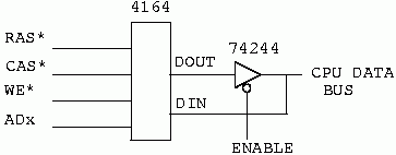
In figure 6 we see our 4164 implemented for separate data in and out pins. The key to this circuit is the enable. The 74244 buffer is only enabled during read operations. During writes, this buffer is left disabled. Thus, the data present at it's DOUT pin remains isolated from the CPU data bus. The new data is written into the device by the pulse on WE.
I once used this circuit to implement a 10 MHz Z8000 CPU card with 150ns. memories, and no wait states. With common early write, it would have required 100 ns memories, and one wait state for writes.
OK. What is early write, and why would I want it. It sounds like it would cost performance. Well, it does. But, we have to learn how to deal with it because all the SIMM modules use it, as do the new byte and word wide DRAMS that are coming out. Separate I/O is nice, but it uses too many package pins. On SIMM modules, where data may be 8, 9, 32, or 36 bits wide, there is no room on the connector for separate in and out pins. The same is true on the byte and word wide parts.
So, that said, let's look at early write. On these denser parts package pins are conserved by tying the in and out pins together and using a single pin as a bi-directional data pin. On some SIMM modules, they literally tie two package pins together on that tiny printed circuit board. Looking at figure 5 it is obvious that we can no longer use the read-modify-write cycle. It allows the output to be turned on, which would conflict with the data your CPU is trying to write. Not good. What we need is a way to tell the DRAM chip that we really aren't doing a read, and not to turn its' output on. This would eliminate the conflict.
The way we do this is by taking WE low before we take CAS low. If WE is low when CAS goes low the DRAM will not turn on its' outputs. Yes, there is a catch to it. The data is written into the device AS CAS GOES LOW. This means that you must somehow hold off CAS for write cycles until you know that the data is valid. On some processors this means that you will need a wait state on writes. Since you had to wait till later in the cycle to activate CAS, it may take you longer to complete the memory cycle. How many of your 486 motherboards require a wait state on memory writes? It is very common for just this reason. The timing of an early write cycle looks like this.
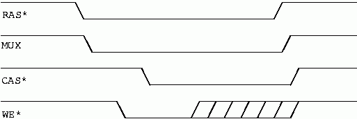
In figure 7 we see an early write cycle. Note that CAS is held off until after WE is low. How you will implement this in hardware will depend on the processor you are using. We said we were considering the Z80 so we will look at how one might implement this on a Z80. The following circuit should generate the needed signals. It is shown as discrete gates to illustrate the logic. It would be very cleanly implemented in a PAL, or Programmable Array Logic device.
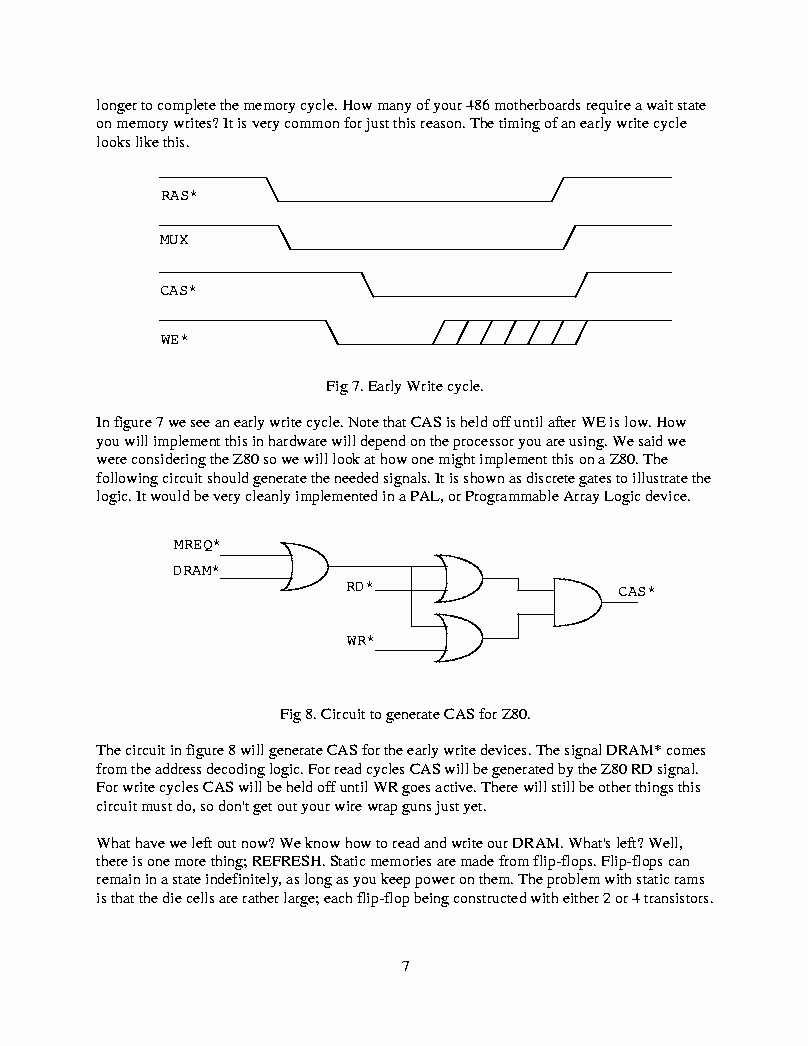
The circuit in figure 8 will generate CAS for the early write devices. The signal DRAM* comes from the address decoding logic. For read cycles CAS will be generated by the Z80 RD signal. For write cycles CAS will be held off until WR goes active. There will still be other things this circuit must do, so don't get out your wire wrap guns just yet.
What have we left out now? We know how to read and write our DRAM. What's left? Well, there is one more thing; REFRESH. Static memories are made from flip-flops. Flip-flops can remain in a state indefinitely, as long as you keep power on them. The problem with static rams is that the die cells are rather large; each flip-flop being constructed with either 2 or 4 transistors.
In dynamic memories, the storage element is a capacitor. Just put a charge into the capacitor for a one, take it away for a zero. The problem with capacitors is that they won't hold their charge forever. At least not without some help they won't. The reason capacitors won't hold their charge is something called leakage. The charge is held on two plates, one with a positive charge, one with a negative charge. The plates are held apart with some kind of insulator, or dielectric. Charge leaks between the plates through the dielectric. Now, wouldn't it be great if we put our program in one of these capacitors, then came back a little later to run it, and it wasn't there anymore? That is exactly what DRAMs would do without refresh.
Someone smarter than me decided that if you were to periodically go around to all of the capacitors and freshen up the charge, that this just might work. Well, it does. To refresh a DRAM you must reference every row address in the device within a specified amount of time. As DRAM devices get denser, that is bigger, they have more rows in them. The 4164 we've been talking about has 256 rows; it uses 8 bits for the row address. A modern 4MB part has 2048 rows, using 11 bits for the row address. This is eight times as many rows. If we had to refresh all rows in any device in the same amount of time, then with the 4MB part, we would need to run refresh eight times as fast as for the 4164, just to get through in time.
Fortunately, this is not true. Over the years chip manufacturers have gotten the leakage performance of each successive part a little better. Now we can basically refresh each part at the same rate as the last one. This is good. If we had to keep refreshing faster and faster, we would soon have no bandwidth left for the CPU to use the memory. We would be using all the available time to refresh it.
OK. How do we do this thing called refresh? Glad you asked. There are two ways of doing it; RAS only refresh, and CAS before RAS refresh. Let's examine RAS only refresh first.
Examining figure 9 we see that a RAS only refresh consists of providing a row address, and strobing RAS. CAS and WE must be held high during this cycle. It is CAS remaining high that tells the device that this is a refresh cycle. In DRAMS it is CAS that controls the output drivers. By keeping CAS high, the output drivers remain off, and the row which was accessed is refreshed.
Actually, every read cycle is also a refresh cycle for the row accessed. The problem with normal reads is that they tend to be random. You cannot guarantee that all possible row addresses will be referenced in the specified time just by executing programs. Therefore, we must refresh the device. The Z80 CPU provides a mechanism for refreshing DRAMs. Unfortunately for us, the Z80 was designed just before the last ice age; when 4116 (16K by 1) DRAMs were popular. Thus, they only furnish 7 bits of refresh address. The intent of this refresh mechanism was to support the RAS only refresh. At that time, that was all we had, and if you are going to work with the 4164, that is what you MUST implement. CAS before RAS hadn't come along yet. This is a bummer, but we can still use the Z80's refresh cycle to control refresh, we just have to furnish the address. A RAS only refresh DRAM subsystem may be implemented as shown in the following illustration.
We are rapidly approaching our promised design implementation for the Z80. The circuit in figure 10 will implement a single row of 4164, 64K by 1, DRAMs for the Z80. Don't worry, when we're done, we will draw a MUCH better diagram for you. There are a few control issues left out of figure 10 for the sake of simplifying the drawing.
RAS only refresh was the only thing we had to work with until the arrival of the 256K by 1 devices. With the 256K devices we got CAS before RAS refresh. and NOT ALL OF THEM HAD IT. If you are designing with 256K parts, you should consult the manufacturers data sheet for the parts you want to use to verify that they support CAS before RAS refresh. If not, you must either implement RAS only refresh, or find some other parts.
Ok. What does CAS before RAS refresh look like? Let's see.
Oh boy. This looks different. We are used to seeing RAS go active before CAS. Also, we now don't care about what is on the address lines. WE must be held high during the refresh cycle, and that's it. Done. This really looks simple, but what does it do for us in hardware? Let's see.
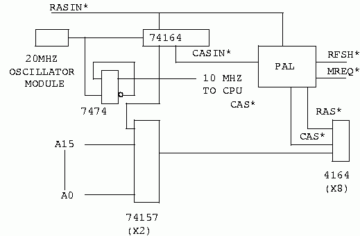
This looks suspiciously like figure 4. It is, with the addition a PAL, or Programmable Array Logic, device. At this point, the PAL makes implementation of this kind of logic MUCH easier. The equations for RAS and CAS in figure 12 would look something like this.
/RAS = /MREQ * RFSH * /RASIN      ; NORMAL RAS

   + /MREQ * /RFSH * /CASIN   ; REFSRESH

/CAS = /MREQ * RFSH * /CASIN  ; NORMAL CAS
   + /MREQ * /RFSH * /RASIN   ; REFRESH
From the above equations it becomes quite clear how CAS before RAS refresh works. We still have our shift register generating the timing for us. For a normal memory cycle, we pass this on through. But, for a refresh cycle, we swap the outputs. The signal that is normally RAS goes to CAS, and the signal that is normally CAS goes to RAS. This implements the CAS before RAS function very nicely. The processor will hold WR high during a refresh cycle, so there we are. The only thing left for us to do is to add in RD and WR. You did remember that we have to hold off CAS for writes didn't you? Of course you did. The new equations would look like this.
/RAS = /MREQ * RFSH * /RASIN      ; NORMAL RAS
       + /MREQ * /RFSH * /CASIN   ; REFSRESH

/CAS = /MREQ * RFSH * /CASIN * /RD   ; NORMAL CAS FOR READ
      + /MREQ * RFSH * /CASIN * /WR  ; NORMAL CAS FOR WRITE
      + /MREQ * /RFSH * /RASIN       ; REFRESH
The memory subsystem shown in figure 12 may be implemented with any DRAM device that supports CAS before RAS refresh. With the equations above, you can also support early write and use devices with a bi-directional data pin. Before we move on, let's examine some of these devices that might be of interest.
When trying to build a project with the fewest components we might want to examine some of the denser parts. One such part is the 64K by 4 DRAM. It is/was available from several vendors. It may not be currently being made any more, but you may find them in the surplus channels. I have personally removed several of them from old 286' machines. with 2 of these parts, you have 64K of memory for a Z80. They are new enough to support CAS before RAS refresh, and the use early write. The device looks like this.
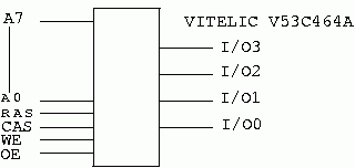
The chip shown in figure 13 has one pin we haven't discussed yet; OE. This pin may be tied to ground and ignored. This device is really a 256K bit part internally. They just arranged it as four banks of 64K.
The move to make DRAMs wider than one bit is becoming a welcome trend. There are now parts that are 8, 9, 16, 18 bits wide. Let's look at another device that is 8 bits wide. Perfect for the Z80 except that it is greater than 64K. We will discuss memory management on the Z80 later. The device we will discuss next is the Vitelic V53C8256H.
NOTE : I am using a MOSEL/VITELIC data book for some of these parts because it is what I have handy. Most, or all. of these decices are manufactured by many different memory vendors. Consult the appropriate data book. I have especially concentrated on the older devices as I felt that they would be available on the surplus market at good prices. Or, turn over that pile of old XT and 286 motherboards, and see what gold lies there.
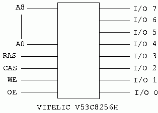
With the chip in figure 14 you would have a 256KB memory system in one chip. This trend goes on with the current highest density device being 2M by 8, I believe; and in one chip. Of course these are the current state of the art devices, and you will have to pay real money for them. The older devices can be had for free, or very close to it.
Let's examine one more memory system design issue before we move on to memory management; parity. Should we or shouldn't we have parity? That is a question that only you can answer. It depends on the application. Most applications probably don't need parity, but some do. Medical applications, or anything that needs to be fail safe should have AT LEAST parity, if not ECC. All parity will do is tell you that something happened, not how to fix it.
Parity is a wonderful thing if you are a DRAM manufacturer. You just found a way to sell every customer more of your product. All you have to do is create a panic in the user community. Make them believe that their memory is so unreliable that they need this, then you will be able to sell them more of it. But, if the manufacturers memory is that unreliable, why are we buying it in the first place? OK. I'll get down off my soapbox. If you think you really need parity, then read on.
What is parity anyway. Well, put simply, it forces the number of bits set to a one across the stored word, including the parity bit, to be either even, or odd. For example, consider that the data on the CPU's data bus is 00001111. To implement an even parity system, we would store a zero in the parity bit. The byte we are generating parity for is already even since it has four bits set to a one. By storing a zero in the parity bit, we still have an even number of bits set to a one. If we were implementing an odd parity system, we would store a one in the parity bit for this example. We would then have odd parity across all nine bits of the stored data.
I prefer to implement odd parity for DRAM systems. This ensures that there will be at least one bit in the group that is set to a one. Very often DRAM will come up with all zeroes in it after power up. If we implemented even parity we could read uninitialized memory, and not detect it.
To add parity to your system you need to add one more ram chip to each byte. Since we are talking about a Z80 processor, and it is only an 8 bit processor, we will add one ram chip to each row of memory. A special circuit manages that extra device. It gets the same RAS, CAS, and WE as the rest of that row of devices, but it's data doesn't come from the data bus. Consider the following.
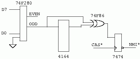
The heart of the implementation of parity is the 74F280 device. It watches the data on the Z80's data bus and continuously generates the parity of it. The 74F280 is very fast. It will typically generate parity in 4 to 5ns. While this is fast we must remember to include this time in our speed calculations when we get to the application of all this theory.
The design in figure 15 uses a part with separate I/O pins for the parity device. If we didn't, we would have to insert a tristate buffer between the memory and the 74F280, then add control logic to decide when to enable it. We would also have another delay between the output of the 74F280 and the memory.
During a write cycle the parity is written into the parity ram. When the data is read back out of memory and placed on the CPUs data bus, the 74F280 generates the parity on the data just read back. The results are fed to the 74F86 XOR gate along with the value read back from the parity ram. If they are both the same there will be a zero on the output of the XOR gate. This value is sampled at the end of the memory cycle when CAS goes back high. If the generated parity does not agree with the parity stored in the extra ram an interrupt will be generated. System software will then have to figure out what to do about it.
The 30 pin SIMM modules were designed with parity in mind. And here you thought I was going to forget SIMM modules. Let's look at a 4MB by 9, 30 pin, SIMM module.
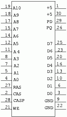
Figure 16 is shown as a data sheet because I have seen repeated requests for the pinout of a SIMM on the internet. If you hold the module in your hand with the chips facing up,. and the edge connector facing you, then pin 1 in on the left end. You may treat this module just the same as you would the 256K by 8 device in figure 14.
Note that the 8 data lines are bi-directional, but the parity bit has separate I/O pins. The parity bit also has a separate CAS pin. This is usually tied to the primary CAS pin for the module. If you wanted to delay the write to the parity chip, to allow ,more time for the parity to be valid, you could generate a separate CAS signal for it. In practice this is usually not necessary. The parity circuit in figure 15 will handle the parity bit quite nicely.
For a number of reasons 30 pin SIMMs should be seriously considered for any home-brew project. Using a SIMM module may spell the difference between success and not success for your project; especially if it is hand wired. The SIMM module already has a PCB with the DRAMs mounted on it. It also has the correct bypass capacitors mounted under the DRAM chips. This gives you a step up on the most difficult part of implementing DRAMs in a prototype environment; power distribution.
Another reason for considering using 30 pin SIMM modules is that the industry is moving on to the 72 pin modules. it is now fairly easy to find 256K, 30 pin, SIMMs cheap. One surplus store near me has them for $3.95 each. The 1MB and up parts are still in demand, and the price on them is actually going up. Oh well. That's what supply and demand will do for you. We will not discuss the 72 pin modules here. They are 32 bits wide. Our stated goal was to interface memory to a Z80 which is 8 bits wide. While we could implement the module as four banks of 8 bit memory this is kind of esoteric and we won't do it. Should I get a flood of requests, we'll see.