 11.0
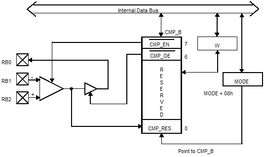
COMPARATOR The device contains an on-chip differential comparator. Ports
RB0-RB2 support the comparator. Ports RB1 and RB2 are the comparator negative
and positive inputs, respectively, while Port RB0 serves as the comparator
output pin. To use these pins in conjunction with the comparator, the user
program must configure Ports RB1 and RB2 as inputs and Port RB0 as an output.
[Bean says: "When you enable the comparitor RB.0 is always an output and
RB.1 & RB.2 are alway inputs. Even if you try to change them AFTER the
comparitor is enable they don't change."] The CMP_B register is used
to enable the comparator, to read the output of the comparator internally,
and to enable the output of the comparator to the comparator output pin.
11.0
COMPARATOR The device contains an on-chip differential comparator. Ports
RB0-RB2 support the comparator. Ports RB1 and RB2 are the comparator negative
and positive inputs, respectively, while Port RB0 serves as the comparator
output pin. To use these pins in conjunction with the comparator, the user
program must configure Ports RB1 and RB2 as inputs and Port RB0 as an output.
[Bean says: "When you enable the comparitor RB.0 is always an output and
RB.1 & RB.2 are alway inputs. Even if you try to change them AFTER the
comparitor is enable they don't change."] The CMP_B register is used
to enable the comparator, to read the output of the comparator internally,
and to enable the output of the comparator to the comparator output pin.
The comparator enable bits are set to “1” upon reset, thus disabling the comparator. To avoid drawing additional current during the power down mode, the comparator should be disabled before entering the power down mode. Here is an example of how to setup the comparator and read the CMP_B register.
	mov	M,#$08 	;set MODE register to access
			;CMP_B
	mov   	W,#$00 	;clear W
	mov   	!RB,W 	;enable comparator and its
			;output

	... 		;delay after enabling
			;comparator for response

	mov   	M,#$08 	;set MODE register to access
			;CMP_B
	mov   	W,#$00 	;clear W
	mov   	!RB,W 	;enable comparator and its
			;output and also read CMP_B
			;(exchange W and CMB_B)
	and   	W,#$01 	;set/clear Z bit based on
			;comparator result
	snb   	$03.2 	;test Z bit in STATUS reg
			;(0 => RB2<RB1)
	jmp   	rb2_hi 	;jump only if RB2>RB1
The final “mov” instruction in this example performs an exchange of data between the working register (W) and the CMP_B register. This exchange occurs only with Port B accesses. Otherwise, the “mov” instruction does not perform an exchange, but only moves data from the source to the destination.
CMP_B: Comparator Register (MODE=08h)
When you access the CMP_B register using MOV !RB,W, the CPU does an exchange
between the contents of W and CMP_B. This feature lets you read the CMP_B
register contents. Clear bit 7 to enable operation of the comparator. Clear
bit 6 to place the comparator result on the RB0 pin. Bit 0 is a result bit
that is set to 1 when the voltage on RB2 is greater than RB1, or cleared
to 0 otherwise.
Tracy Allen wrote:
Here are results of tests on one SX28. Maybe these observations can be of use to others.
Schmitt trigger inputs, testing for lower and upper threshold, V0 and V1.Test done with 10kohm potentiometer from Vdd to Vss, with 10uf capacitor on the wiper.
* Vdd = 5 volts
- test on rb1:  V0=0.95 volts,  V1=3.43 volts   (note not symmetrical wrt Vdd/2)
- test on rb2:   V0=1.15 volts,  V1= 3.51 volts  (i.e., small variations pin to pin)

* Vdd = 4.2 volts
- test on rb2:  V0=0.75 volts,  V1=3.05 volts

* Vdd = 3.0 volts
- test on rb2:  V0=0.6 volts,  V1=2.1 volts
The Schmitt thresholds do not depend on the setting in the LVL register (CMOS vs TTL)--The Schmitt trigger is a separate signal path.
Comparator threshold common mode input range, SX28.CMP_B register set to zero to enable comparator action with feedtrough to rb0 output.
Test done with 10k pots from Vdd to Vss as above, one for rb1 and one for rb2.* Vdd = 5 volts - Comparator worked from less than 0.05 up to 4.9 volts. However, the offset degrades at the extremes, at the high end especially. For example, with rb2 = 1.5 volts, switching occurred at rb1 = 1.51 volts, a 10 millivolt offset. At rb2 = 4.8 volts, switching occurred at rb1 = 4.57 volts, a 230 millivolt offset. Above 4.9 volts there was no comparator action. * Vdd = 3 volts - Comparator functioned from less than 0.05 volt up to a little less than 2.8 volts. The offset degraded above 2 volts.
Comparator response time:Test done by connecting rb0 (comparator output) to rb1 (comparator inverting input) and a voltage source (potentiometer) to rb2 (comparator non-inverting input). This turns the comparator into an oscillator with a period determined by the propagation delay. Observe the effect of varying the voltage Vref on the (+) input. That changes the oscillator period (indirectly measuring the propagation delay).
* Vdd = 5 volts
- minimum period, 42 nanoseconds, when Vref=1.3 volts
- period stays in the range of 42 to 60 nanoseconds for Vref in the range of 0.1 volt to 3.8 volt
- period lengthens and degrades rapidly above 3.8 volts and below 0.1 volts

* Vdd = 3 volts
- minimum period, ~60 nanoseconds, from Vref=0.9 to 1.5 volts
- period at Vref=0.1 volt is 75 nanoseconds, 195 nanoseconds at Vref=0.03 volts.
- period at Vref=1.9 volts is 90 nanoseconds, degrades rapidly above 2 volts.
RB.0 Read Comparator SpeedBit 0 in the CMP_B register follows the result of the compare (and is synced with the processor clock). I wanted to check its speed. I hooked rb.7 up to rb.1 and left rb.2 hooked up to a variable voltage (potentiometer, Vss to Vdd). The program sets rb.7, reads the CMP_B register, and transfers rb to rc. Like this:
   mode #$08
  mainloop
  setb rb.7     ; comparator input high
  mov !rb,#$00  ; exchange cmp_b with w
  mov rc,w     ; this sets rc.0 equal to bit0 of CMP_B
   clrb rb.7   ; comparator input low
   mov !rb,#$00    ; get CMP_B
   mov rc,w       ; sets rc.0 equal to bit0 of CMB_B
  jmp mainloop
My thought was that at high clock speeds, reading CMP_B immediately after toggling the comparator input might not leave enough time for the bit to propagate through into the bit0 of CMP_B. For this test, the 'scope was triggered by rb.7, the comparator input, and a second probe tested rc.0, which should follow the value of the CMP_B result bit. Looking at the data sheet, where it claims a 250 nanosecond propagation time, I was thinking I might have to insert a NOP or two or more in between setting the comparator input and reading the result. But no, it turns out that even with a 50 megahertz clock, the result appears on rc.0 three clock cycles after the input toggles. And that was true for input levels from 0.04 volts up to 4.2 volts.
I haven't tested it yet with smaller input overdrives, or with a 3 volt Vdd, but I was pleasantly suprised by the input range and by the speed.
Current Drain in SLEEP mode
The SX docs suggest that the comparator module should be disabled in SLEEP in order to minimize current drain. However the data sheet does not expand on that point. That is an important parameter for micropower apps.
Here is a rundown from experiment, where I applied voltage from two poteniometers to the comparator inputs, rb1 and rb2, and then put the chip into eternal SLEEP. (Caveat--observations based on one SX28 chip).
The minimum comparator active current drain is about 110 microamps.
-- both inputs must be near either Vss or Vdd
-- the two inputs must be separated by a certain voltage--20 millivolts is enough.
The current drain increases to ~1 milliamp when the two input voltages are equal (allowing for the input offset voltage), _and_ both near the rails. For example, both are at 0.1 volt or both are at 3.5 volts. The current is difficult to measure, as there is a tendency for self oscillation, 60hz pickup, etc.etc, when near the switching point.
The surprising thing comes when either comparator input is near 1.8 volts, while the other one is near the rails. The current drain is around 2.5 milliamps. The current drain peak is narrow around that threshold. The current drain profile as a function of input voltage is pretty much the same as the profile when the comparator is disabled (That is why we never want to leave inputs floating!).
If both inputs of the comparator are near the 1.8 volt level, the current drain can be as high as 4.5 milliamps, even if the voltage difference is enough to keep the comparator output solidly in one state or the other.
The lesson here for anyone wanting to use the comparator and at the same time to minimize current drain, would be to keep the input voltage levels below 1.3 volts (or above 2.3 volts), and, to include at least 20 mV of hysteresis.
Bean says:
When you enable the comparitor RB.0 is always an output and RB.1 & RB.2 are alway inputs. Even if you try to change them AFTER the comparitor is enable they don't change.
| file: /Techref/scenix/analogcomparator.htm, 9KB, , updated: 2007/12/7 17:49, local time: 2025/11/1 02:19,
owner: zizaidi-g_c_t-,
216.73.216.123,10-1-33-36:LOG IN
|
| ©2025 These pages are served without commercial sponsorship. (No popup ads, etc...).Bandwidth abuse increases hosting cost forcing sponsorship or shutdown. This server aggressively defends against automated copying for any reason including offline viewing, duplication, etc... Please respect this requirement and DO NOT RIP THIS SITE. Questions? <A HREF="http://www.massmind.org/Techref/scenix/analogcomparator.htm"> SX Embedded Controller Analog Comparator module</A> |
| Did you find what you needed? |
Welcome to massmind.org! |
|
The Backwoods Guide to Computer Lingo |
.