This application note presents programming techniques for producing a programmable output voltage by smoothing a pulse width modulated (PWM) digital output with a simple resistor-capacitor low-pass filter, and essentially creating a digital to analog converter. This implementation uses the SX's internal interrupt feature to allow background operation of the code as a virtual peripheral, and uses the Parallax demo board, taking advantage of Parallax' SX demo software user interface and UART features to allow the SX to communicate simply and directly with a personal computer via a serial RS232C port.
;******************************************************************************
;       Virtual Peripheral: Pulse Width Modulators
;
;
;       Length: 36 bytes (total)
;       Authors: Chip Gracey, President, Parallax Inc.
;		   modified by Craig Webb, Consultant to Scenix Semiconductor, Inc.
;       Written: 97/03/10 to 98/6/03
;
;******************************************************************************
;
;****** Assembler directives
;
; uses: SX28AC, 2 pages of program memory, 8 banks of RAM, high speed osc.
;       operating in turbo mode, with 8-level stack & extended option reg.
;
		DEVICE  pins28,pages2,banks8,oschs
		DEVICE  turbo,stackx,optionx
		ID      'PWMS'			;program ID label
		RESET   reset_entry             ;set reset/boot address
;
;******************************* Program Variables ***************************
;
; Port Assignment: Bit variables
;
pwm0_pin        EQU     rc.0                    ;Pulse width mod. PWM0 output
pwm1_pin        EQU     rc.2                    ;Pulse width mod. PWM1 output
;
;****** Register definitions (bank 0)
;
		org     8                       ;start of program registers
main            =       $                       ;main bank
;
temp            ds      1                       ;temporary storage
byte            ds      1                       ;temporary UART/I2C shift reg.
flags           DS      1                       ;program flags register
;
delay1		DS	1			;temporary delay variable
delay2		DS	1			;temporary delay variable
;
		org     50h                     ;bank2 variables
analog          =       $                       ;pwm and ADC bank
;
port_buff       ds      1                       ;buffer - used by all
pwm0            ds      1                       ;pwm0 - value
pwm0_acc        ds      1                       ;     - accumulator
pwm1            ds      1                       ;pwm1 - value
pwm1_acc        ds      1                       ;     - accumulator
;
;
int_period	=       163                     ;period between interrupts
;
;**************************** INTERRUPT CODE *******************************
;
; Note: The interrupt code must always originate at 0h.
;       Care should be taken to see that any very timing sensitive routines
;       (such as adcs, etc.) are placed before other peripherals or code
;       which may have varying execution rates (like the UART, for example).
;
interrupt       ORG     0                       ;interrupt starts at 0h
;
;
;***** Virtual Peripheral: Pulse Width Modulators
;
; These routines create an 8-bit programmable duty cycle output at the
; respective pwm port output pins whose duty cycle is directly proportional
; to the value in the corresponding pwm register. This value is added to an
; accumulator on each interrupt pass interrupt. When the addition causes a
; carry overflow, the ouput is set to the high part of its duty cycle.
; These routines are timing critical and must be placed before any
; variable-execution-rate code (like the UART, for example).
;
;       Input variable(s) : pwm0,pwm0_acc,pwm1,pwm1_acc
;       Output variable(s) : pwm port pins
;       Variable(s) affected : port_buff, pwm0_acc, pwm1_acc
;       Flag(s) affected : none
;	Size : 2 bytes + 4 bytes (per pwm)
;		+ 2 bytes shared with adc code (see below)
;       Timing (turbo) : 2 cycles + 4 cycles (per pwm)
;			 + 2 cycles shared with adc code (see below)
;
:set_analog	bank    analog                  ;switch to adc/pwm bank
		clr     port_buff               ;clear pwm/adc port buffer
;
:pwm0           add     pwm0_acc,pwm0           ;adjust pwm0 accumulator
		snc                             ;did it trigger?
		setb    port_buff.0             ;yes, toggle pwm0 high
:pwm1           add     pwm1_acc,pwm1           ;adjust pwm1 accumulator
		snc                             ;did it trigger?
		setb    port_buff.2             ;yes, toggle pwm1 high

:update_RC	mov     rc,port_buff            ;update cap. discharge pins
;
		mov     w,#-int_period          ;interrupt every 'int_period' clocks
:end_int	retiw                           ;exit interrupt
;
;******	End of interrupt sequence
;
;***************************** SUBROUTINES *********************************
;
;***************************** MAIN PROGRAM CODE ******************************
;
;		ORG     100h
;
; Program execution begins here on power-up or after a reset
;
reset_entry
		clr     rc                      ;initialize port RC
		mov     !rc,#%10101010          ;Set RC in/out directions
		mov     m,#$D                   ;set input levels
		mov     !rc,#0                  ; to cmos on port C
		mov     m,#$F                   ;reset mode register
		CLR     FSR                     ;reset all ram starting at 08h
:zero_ram       SB      FSR.4                   ;are we on low half of bank?
		SETB    FSR.3                   ;If so, don't touch regs 0-7
		CLR     IND                     ;clear using indirect addressing
		IJNZ    FSR,:zero_ram           ;repeat until done

		mov     !option,#%10011111      ;enable rtcc interrupt
;
; Main Program Loop
;
:loop		DJNZ	delay1,:loop		;do inner delay loop
		DJNZ	delay2,:loop		;do outer delay loop
		INC	pwm0			;increase pwm0 - ramp output
		DEC	pwm1			;decrease pwm1 - sawtooth output
;
; <program code goes here>
;
		JMP     :loop                   ;back to main loop
;
;***************
		END                             ;End of program code
| 1 The duty cycle is the proportion of time which the signal is high or active (i.e. charging the capacitor) |
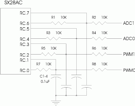
The circuit is a simple resistor capacitor network (R5&C1 for pwm0, R7-C2 for pwm1) on each pwm port pin (see figure 1), which acts as a low-pass filter and smoothes the oscillating digital signal output so that it appears as a linear voltage whose value is determined by the duty cycle1 of the signal, which is directly controlled by the 8 bit value in the pwm register.
The interrupt code segment is quite straight forward. The pwm value is added to an accumulator register during each pass through the interrupt and the pwm output is set to high every time the accumulator overflows. This technique allows the eight bit value in the pwm register to directly set the duty cycle of the pwm signal output and hence directly control the voltage on the capacitor.
| 2 The 3 dB point is the frequency at which the filter cuts the incoming signal level by 50% (to ½ it's original value). For a low-pass filter, signals at frequencies higher than the 3 dB point are attenuated even further. |
With the resistor and capacitor values shown, the corner frequency or 3 dB point2 for the low-pass filter is calculated as follows:
frequency3dB = 1 / (2 * p * R * C ) = 1 / (2 * 3.1416 * 10kW * 0.1uF) = 159 Hz
| 3 With a pwm value of 1, there will only be one carry generated every 256 passes by adding the pwm value to the pwm accumulator. In the case of a pwm value of 0FFh, only 1 of every 256 passes won't generate a carry (and hence a low at the pwm output). |
In order to generate a fixed voltage from the pwm output from the changing digital pwm signals, a low-pass filter must be used whose corner frequency is lower than the lowest frequency component of the digital pwm signal. The length of the pwm cycle varies, depending upon the value in the corresponding pwm register, but the worst case is a pwm value of either 1 or 0FFh, in which case 256 interrupt passes are required to complete the pwm cycle3. We can calculate the period between interrupt passes as follows:
| * The interrupt is triggered each time the RTCC rolls over (counts past 255 and restarts at 0). By loading the OPTION register with the appropriate value, the RTCC count rate is set to some division of the oscillator frequency (in this case they are equal), which is the external 50 MHz crystal in this case. At the close of the interrupt sequence, a predefined value is loaded into the W register using the RETIW instruction which determines the period of the interrupt in RTCC cycles. |
period (sec) = mode * prescaler * RETIW value* / osc. frequency, where mode=1 (turbo) or =4 (normal)
So, for the worst case of 256 interrupt passes, at a crystal frequency of 50 MHz, in turbo mode, with a prescaler of 1, and with an RETIW value of 163, the lowest frequency present in the pwm signal is:
frequencymin = 1 / period * 256 = 50 MHz / (1 * 1 * 163 * 256 ) = 1.2 kHz
By this we can see that the pwm signal will be excellently smoothed by the resistor and capacitor values chosen, since the lowest frequency component possible is well above the corner frequency for the low-pass filter.
| 4 The charging and discharging times are calculated similarly. |
The only inconvenience that the low-pass filter causes is that it also limits the pwm's output settling time (i.e. the maximum frequency and linearity if the pwm is being used as a signal generator). With the RC values shown, the settling time is calculated from the equation V=Vcc (1-e-t/RC ) for the charging4 voltage on the capacitor after time t. If we want to calculate the settling time to eight bit resolution, we have:
V = Vdd (28 - 1) / 28 = Vdd ( 1 - e-t/RC ) so: ln(1/ 28 ) = -t / RC
therefore: tsettle = - RC * ln(1 / 28 ) = - 10kW * 0.1uF * ln(1 / 28 ) = 5.5 msec
| 5 In practise, circuit noise is usually larger than the 8-bit resoltion of the pwm, so that the settling time can be considered as somewhat less than the calculated value |
So, with the above RC values, a maximum frequency of fmax = 1/ tsettle = 1 / 5.5 ms = 180 Hz is possible on the pwm outputs for signals that vary if eight bit resolution is required5.
The second 10kW resistor attached to each pwm output (i.e. R6 and R8), acts as a current limiting resistor to avoid discharging the voltage stored on the capacitor in case the output is driving a source which doesn't have a high input impedance. Ideally, the input impedance of the circuit being driven is at least a couple orders of magnitude larger (i.e. >= 1MW) than this resistor value so that the voltage on the capacitor remains accurate.
| 6 for the 4th pwm output pwm0 should be relaced with pwm3, pwm0_acc with pwm3_acc, and port_buff.0 with port_buff.6 |
The Parallax demo board is designed so that port pins adc0 and adc1 can be swapped for pwm's simply by adjusting the program code. To do this (if you'd like 1-2 more pwm outputs) requires commenting out (or removing) the adc code section, and reproducing the three lines of pwm0: code once (or twice for two more pwm outputs), while replacing pwm0 with pwm2, pwm0_acc with pwm2_acc, port_buff.0 with port_buff.4 6 in the three code lines. New register definition(s) should also be added in the analog bank for pwm2 & pwm2_acc (and pwm3 & pwm3_acc, if required). An example follows:
...
analog 		= 	$ 		;pwm bank
;
port_buff 	ds 	1 		;buffer - used by all
pwm0 		ds 	1 		;pwm0 - value
pwm0_acc 	ds 	1 		; - accumulator
pwm1 		ds 	1 		;pwm1 - value
pwm1_acc 	ds 	1 		; - accumulator
pwm2 		ds 	1 		;pwm2 - value
pwm2_acc 	ds 	1 		; - accumulator
pwm3 		ds 	1 		;pwm3 - value
pwm3_acc 	ds 	1 		; - accumulator
...
:pwm0 		add 	pwm0_acc,pwm0	;adjust pwm0 accumulator
		snc 			;did it trigger?
		setb 	port_buff.0 	;yes, toggle pwm0 high
:pwm1 		add 	pwm1_acc,pwm1 	;adjust pwm1 accumulator
		snc 			;did it trigger?
		setb 	port_buff.2 	;yes, toggle pwm1 high
:pwm2 		add 	pwm2_acc,pwm2 	;adjust pwm2 accumulator
		snc 			;did it trigger?
		setb 	port_buff.4 	;yes, toggle pwm2 high
:pwm3 		add 	pwm3_acc,pwm3 	;adjust pwm3 accumulator
		snc 			;did it trigger?
		setb 	port_buff.6 	;yes, toggle pwm3 high
;
; <adc code removed except for this one line>
		mov 	rc,port_buff 	;update port pins (port RC)
...
| file: /Techref/scenix/lib/io/osi1/pwm/pwm_vp.htm, 13KB, , updated: 2002/3/12 22:49, local time: 2025/10/16 18:03,
216.73.216.53,10-2-207-162:LOG IN
|
| ©2025 These pages are served without commercial sponsorship. (No popup ads, etc...).Bandwidth abuse increases hosting cost forcing sponsorship or shutdown. This server aggressively defends against automated copying for any reason including offline viewing, duplication, etc... Please respect this requirement and DO NOT RIP THIS SITE. Questions? <A HREF="http://www.massmind.org/Techref/scenix/lib/io/osi1/pwm/pwm_vp.htm"> A Virtual Peripheral DAC: Implementing Pulse Width Modulation</A> |
| Did you find what you needed? |
Welcome to massmind.org! |
Welcome to www.massmind.org! |
.