


Next: Transistor Circuits
Up: Diode Circuits
Previous: Diode Protection
-
- Make a sketch showing the current through an ideal diode as a
function of the applied voltage. Also sketch the current
through a real signal diode as a function of voltage.
- Make a sketch showing the current drawn through a Zener diode as
a function of the applied voltage. Show how to determine the
forward resistance (
 ), the reverse resistance (
  ) and
the Zener resistance (
) and
the Zener resistance (  ) from your sketch. Label the
voltages
) from your sketch. Label the
voltages  and
and  .
.
-
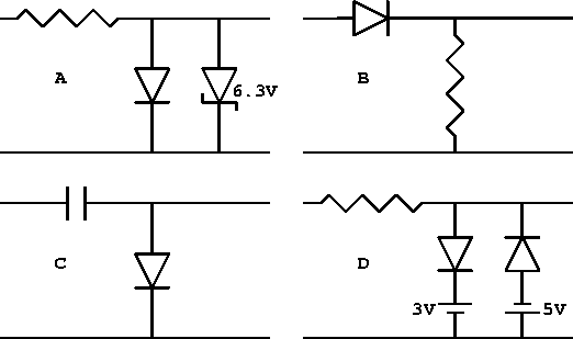
Sketch the expected output waveforms when
- a 100 Hz sine wave with a peak voltage of 5 V, and
- a 100 Hz square wave with a peak-to-peak voltage of 10 V
are applied separately to each of the circuits below.
-
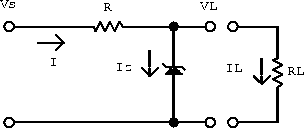
The Zener diode in the following circuit is characterized by
 V and
V and  V. Terminal B is at ground and there
is no external load resistor.
V. Terminal B is at ground and there
is no external load resistor.

- What is the voltage at terminal A in the above circuit?
- What is the current through the Zener? (What reasonable
approximation makes this straightforward?).
- If the Zener is dissipating 1.0
 W (in heat), what can we
conclude to be the effective impedance of the diode for this
situation?
W (in heat), what can we
conclude to be the effective impedance of the diode for this
situation?
-
The effects of a Zener diode in a circuit can be treated analytically
by using an equivalent circuit model of the reverse-biased condition.
In the low voltage region, before breakdown, the Zener diode can be
treated like any other reverse-biased diode.
However, the Zener diode is normally operated in the breakdown region.
- Write down an equivalent linear-circuit model in the breakdown
voltage region.
- Replace the Zener diode in the following voltage reference
circuit by your equivalent circuit model.
- Determine the contribution of the of Zener diode to this voltage
reference circuit by calculating the elements of a Thevenin
equivalent circuit representation.
- Show that for small Zener diode effective resistance the
Thevenin equivalent voltage is close to the Zener breakdown
voltage and thus is insensitive to changes in the source
voltage.
- Show that for small Zener diode effective resistance, the
Thevenin equivalent resistor gives the voltage source a
reasonably small output impedance.
- The combined results show a voltage reference that is
insensitive to voltage changes in the original EMF and to
changes in the load current.
State the assumptions under which this result is valid.
Next: Transistor Circuits
Up: Diode Circuits
Previous: Diode Protection
Doug Gingrich
Tue Jul 13 16:55:15 EDT 1999