What is CPLD ?
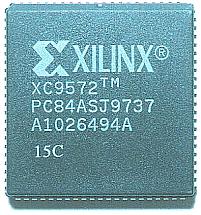
For example, in case of the 7400 IC, 4 circuits of 2 input NAND gate are housed. In case of 7404, 6 circuits of inverter are housed. These are separate IC. Therefore, to compose a circuit, it is necessary to do each wiring among the pins using the printed board. In case of CPLD, it has wiring among the logic in the IC. So, the wiring on the printed board can be made little. 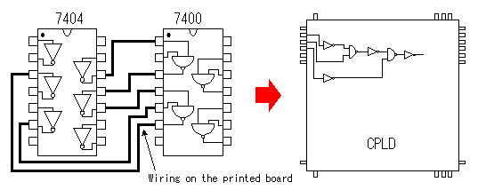 The capacity of CPLD is limited. There is limitation on the number of the pins, too. So, don't do excessive expectations. The outline specification of the part of the XC9500 series of Xilinx Inc. is shown below.
The point which CPLD is convenient for is the thing about which it is possible to rewrite many time because it is recording the contents of the circuit to the flash memory. In the XC9500 series, rewriting in about 10,000 times is said to be possible. Also, because the pin for the rewriting is preparatory, the contents can be rewritten in the condition to have mounted to the actual circuit if there is wiring.
FPGA(Field Programmable Gate Alley) can specify logic inside by the program like CPLD.
|