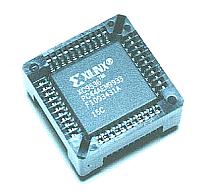
Pin diagrams ( XC9536-PC44/XC9572-PC44 )
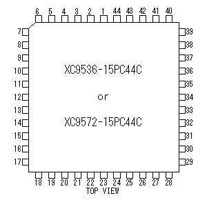 The figure on the left is the top view of CPLD of 44 pins. The following item is used to know the position of the pin.
A pin numbering is counterclockwise given from the center of the line in the topside. Note is necessary to the pin arrangement by the Function Block and the macrocell because it a little irregular-ly. In case of XC9536-PC44, the macrocells which corresponds to the input/output pins are 34 macrocells in the 36 macrocells. In case of XC9572-PC44, they are 34 macrocells in the 72 macrocells. The macrocells which don't correspond to the input/output pins can be used only in the logic circuits inside.
The pins colored purple are pins for JTAG. Pin Diagram of XC9536-15PC44C
Pin Diagram of XC9572-15PC44C
|
||||||||||||||||||||||||||||||||||||||||||||||||||||||||||||||||||||||||||||||||||||||||||||||||||||||||||||||||||||||||||||||||||||||||||||||||||||||||||||||||||||||||||||||||||||||||||||||||||||||||||||||||||||||||||||||||||||||||||||||||||||||||||||||||||||||||||||||||||||||||||||||||||||||||||||||||||||