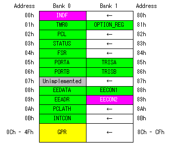
SFR(Special Function Registers) SFR(Special Function Registers)
The first 12 bytes at the head of the RAM file register are used for the SFR. This group of registers is very important to the operation of the PIC. Below I will explain the operation of these registers, which are necessary to the management of the PIC.
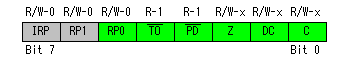
 STATUS Register ( RAM Memory Address 03h,83h ) STATUS Register ( RAM Memory Address 03h,83h ) |
|
 | R = | Readable bit |
| W = | Writable bit |
| -n = | Value at POR reset |
| Bit6,7 = | Unimplemented bit |
|
|
Bit7:
IRP |
Register Bank Select bit(used for indirect addressing)
The IRP bit is not used by the PIC16F84A.
IRP should be maintained clear. |
|
Bit6,5:
RP1,RP0 |
Register Bank Select bit(used for direct addressing)
Only bit RP0 is used by the PIC16F84A.
'0' means Bank0, '1' means Bank1.
RP1 should be maintained clear. |
|
Bit4:
TO(inv) |
Time-out bit
| 1 = | After power-on,CLRWDT instruction,or SLEEP instruction |
| 0 = | Watchdog time-out occurred |
|
|
Bit3:
PD(inv) |
Power-down bit
| 1 = | After power-on or by the CLRWDT instruction |
| 0 = | By execution of the SLEEP instruction |
|
|
Bit2:
Z |
Zero bit
1 =
 | The result of an arithmetic or logic operation is zero |
| 0 = | The result of an arithmetic or logic operation is not zero |
|
|
Bit1:
DC |
Digit carry/borrow(invert) bit (for ADDWF and ADDLW)
| 1 = | A carry-out from the 4th low order bit of the result occurred |
| 0 = | No carry-out from the 4th low order bit of the result |
|
|
Bit0:
C |
Carry/borrow(invert) bit (for ADDWF and ADDLW)
| 1 = | A carry-out from the most significant bit of the result occurred |
| 0 = | No carry-out from the most significant bit of the result occurred |
|
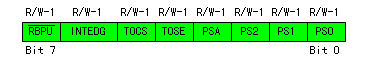
| OPTION_REG Register ( RAM Memory Address 81h ) |
|
 | R = | Readable bit |
| W = | Writable bit |
| -n = | Value at POR reset |
|
|
Bit7:
RBPU(inv) |
PORTB Pull-up Enable bit
| 1 = | PORTB pull-ups are disabled |
| 0 = | PORTB pull-ups are enabled (by individual port latch values) |
|
|
Bit6:
INTEDG |
Interrupt Edge Select bit
| 1 = | Interrupt on rising edge of RB0/INT pin |
| 0 = | Interrupt on falling edge of RB0/INT pin |
|
|
Bit5:
T0CS |
TMR0 Clock Source Select bit
| 1 = | Transition on RA4/T0CKI pin |
| 0 = | Internal instruction cycle clock (CLKOUT) |
|
|
Bit4:
TOSE |
TMR0 Source Edge Select bit
| 1 = | Increment on high-to-low transition on RA4/T0CKI pin |
| 0 = | Increment on low-to-high transition on RA4/T0CKI pin |
|
|
Bit3:
PSA |
Prescaler Assignment bit
| 1 = | Prescaler assigned to WDT |
| 0 = | Prescaler assigned to TMR0 |
|
|
Bit2-0:
PS2-0 | Prescaler Rate Select bits
| PS2 | PS1 | PS0 | TMR0 | WDT |
| 0 | 0 | 0 | 1:2 | 1:1 |
| 0 | 0 | 1 | 1:4 | 1:2 |
| 0 | 1 | 0 | 1:8 | 1:4 |
| 0 | 1 | 1 | 1:16 | 1:8 |
| 1 | 0 | 0 | 1:32 | 1:16 |
| 1 | 0 | 1 | 1:64 | 1:32 |
| 1 | 1 | 0 | 1:128 | 1:64 |
| 1 | 1 | 1 | 1:256 | 1:128 |
|
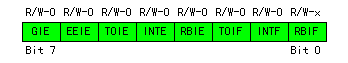
| INTCON Register ( RAM Memory Address 0Bh, 8Bh ) |
|
 | R = | Readable bit |
| W = | Writable bit |
| -n = | Value at POR reset |
|
|
Bit7:
GIE |
Global Interrupt Enable bit
| 1 = | Enables all un-masked interrupts |
| 0 = | Disables all interrupts |
|
|
Bit6:
EEIE |
EEPROM Write Complete Interrupt Enable bit
| 1 = | Enables the EEPROM write complete interrupt |
| 0 = | Disables the EEPROM write complete interrupt |
|
|
Bit5:
T0IE |
TMR0 Overflow Interrupt Enable bit
| 1 = | Enables the TMR0 interrupt |
| 0 = | Disables the TMR0 interrupt |
|
|
Bit4:
INTE |
RB0/INT Interrupt Enable bit
| 1 = | Enables the RB0/INT interrupt |
| 0 = | Disables the RB0/INT interrupt |
|
|
Bit3:
RBIE |
RB Port Change Interrupt Enable bit
| 1 = | Enables the RB port change interrupt |
| 0 = | Disables the RB port change interrupt |
|
|
Bit2:
T0IF |
TMR0 Overflow Interrupt Flag bit
| 1 = | TMR0 has overflow (must be cleared in software) |
| 0 = | TMR0 did not overflow |
|
|
Bit1:
INTF |
RB0/INT Interrupt Flag bit
| 1 = | The RB0/INT interrupt occurred (must be cleared in software) |
| 0 = | The RB0/INT interrupt did not occurred |
|
|
Bit0:
RBIF |
RB Port Change Interrupt Flag bit
| 1 = | When at least one of the RB7:RB4 pins changed state (must be cleared in software) |
| 0 = | None of the RB7:RB4 pins have changed state |
|
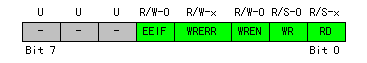
| EECON1 Register ( RAM Memory Address 88h ) |
|
 | R = | Readable bit |
| W = | Writable bit |
| S = | Settable bit |
| U = | Unimplemented bit |
| -n = | Value at POR reset |
|
|
Bit7-5:
Unimplemented | Read as "0" |
|
Bit4:
EEIF |
EEPROM Write Operation Interrupt Flag bit
| 1 = | The write operation completed (must be cleared in software) |
| 0 = | The write operation is not complete or has not been started |
|
|
Bit3:
WRERR |
EEPROM Error Flag bit
| 1 = | A write operation is prematurely terminated |
| 0 = | The write operation completed |
|
|
Bit2:
WREN |
EEPROM Write Enable bit
| 1 = | Allows write cycles |
| 0 = | Inhibits write to the data EEPROM |
|
|
Bit1:
WR |
EEPROM Write Control bit
| 1 = | Initiates a write cycle (The bit is cleared by hardware once write is complete. the WR bit can only be set(not cleared) in software.) |
| 0 = | Write cycle to the data EEPROM is complete |
|
|
Bit0:
RD |
EEPROM Read Control bit
| 1 = | Initiates an EEPROM read (read takes one cycle. RD is cleared in hardware. The RD bit can only be set(not Cleared) in software) |
| 0 = | Does not initiate an EEPROM read |
|
| INDF Register ( RAM Memory Address 00h ) |
|
This register is used when reading from, or writing to, memory by the indirect addressing method.
When reading a memory location by the direct address method, the memory address is directly designated in the instruction code.
movwf 30h is an example of the direct address method
In this case, memory address (30h) is specified in the instruction code and becomes 00 0000 1011 0000 in machine code.
The red part is the instruction code for movwf, the blue part (one bit) specifies a write to the file register, and the green part is the memory address.
In this case, to read or write to a continuous block of memory, an instruction must be written for every memory location. When reading and writing a continuous block of memory, the indirect addressing method is convenient.
When reading and writing a memory location by the indirect addressing method, the memory address is set by the FSR register. The memory contents of the register which was specified by the FSR register is read and written through the INDF register. That is, the INDF register is a relay register for the actual memory.
By incrementing the contents of FSR the contents of the following memory location can be accessed through the INDF. The memory address can be changed by the calculation even if it doesn't make each instruction. You don't need to set up each memory address by instruction. |  |
| EECON2 Register ( RAM Memory Address 89h ) |
|
Writing 55h and then AAh in sequence to the EECON2 enables a data write to the EEPROM register.
Data written to the EEPROM doesn't disappear when power is switched off. Therefore, if the wrong data is written, when the power comes on again, it doesn't return to the original. So, this sequence is used to ensure that when the program is running it does not accidentally write the wrong data to the EEPROM.
An exsample of the correct writing sequence to the EEPROM is shown below.
The red part is the protection sequence.
        bsf     status,rp0      ;Change to Bank1
        bcf     intcon,gie      ;Disables all interrupts
        bsf     eecon1,wren     ;Allows write cycles
        movlw   h'55'           ;Set 55h data
        movwf   eecon2          ;Write 55h to EECON2
        movlw   h'aa'           ;Set AAh data
        movwf   eecon2          ;write AAh to EECON2
        bsf     eecon1,wr       ;Initiates a write cycle
bsf intcon,gie ;Enables all un-masked interrupts |
Configuration Word ( Program Memory Address 2007h )
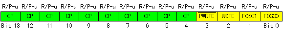 |
| R = | Readable bit |
| P = | Programmable bit |
| -n = | Value at POR reset |
| u = | Unchanged |
|
Bit13-4:
CP |
Code Protection bit
| 1 = | Code protection off |
| 0 = | All memory is code protected |
| |
Code protection is used to prevent the PIC memory contents from being read.
It is set to OFF if reading protection is not needed. |
|
Bit3:
PWRTE(inv) |
Power-up Timer Enable bit
| 1 = | Power-up timer is disabled |
| 0 = | Power-up timer is enabled |
| |
The power up timer maintains the reset condition for about 72 ms after the turning power on.
Generally, it is set to enable. |
|
Bit2:
WDTE |
Watchdog Timer(WDT) Enable bit
| 1 = | WDT enabled |
| 0 = | WDT disabled |
|
Bit1-0:
FOSC1
FOSC0 | Oscillator Selection bits
| FOSC1 | FOSC0 | Oscillator mode | Freq |
| 1 | 1 | Resistor/Capacitor | Less than 1MHz |
| 1 | 0 | High Speed Crystal/Resonator | 4MHz to 20MHz |
| 0 | 1 | Crystal/Resonator | Less than 4MHz |
| 0 | 0 | Low Power Crystal | Less than 200KHz |
|
|