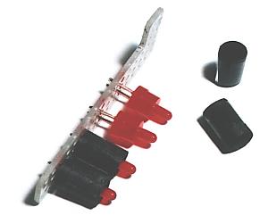
 Modification of the printed circuit board Modification of the printed circuit board
I changed a little the printed circuit board contained in the kit. The modification parts are the LED circuits for the working indication of TM3 and 4.
 Modification of the LEDs for TM3 and 4. Modification of the LEDs for TM3 and 4.
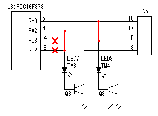
Before modification, LED7 was for true minute indication and LED8 was for true hour indication. The working signal of TM3 and TM4 is output by RA2 and RA3. However, they don't have an LED circuit. Therefore, I modified LED7 for the working display of TM3 and LED8 for the working display of TM4.
Of course, it isn't possible to do an LED display by true minute and true hour. There's no need in the equipment this time.
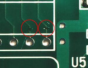 |  |
The pattern of pin13 and pin14 of U3(PIC16F873) is cut. These signals are the true minute and the true hour signal.
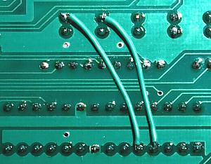
It had better cut a pattern at the part which is near LED7 and LED8. However, it wasn't possible to be cut at there because there was a pattern under the already mounted parts. Because it's not a high frequency circuit, there is no problem. | It wires in the pin4 of U3(PIC16F873) and the anode terminal of LED7 and moreover the pin4 and the anode terminal of LED8. |
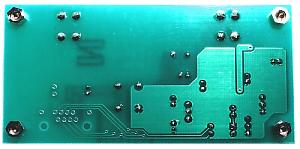
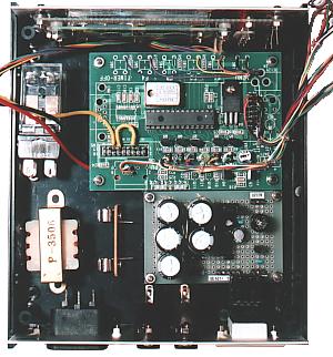
At the beginning, I carried out stack composition of a receiving circuit and a display processing circuit to the design. However, the receiving circuit was very delicate and I turned out that a receiving situation changes with a surrounding radio noise or the directions of a bar antenna. As a conclusion, I decided for a display processing circuit and a receiving circuit to put in a separate case, and to connect them by a cable.
The following modification is the contents at the time of making a receiving circuit and a display processing circuit stack composition. The power supply and the RS232C circuit of a display processing circuit were repealed.
 | 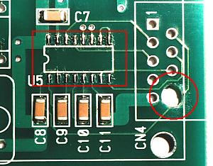 |
| This is a hole for attaching a stud. It has come on a power circuit exactly for the position of the hole of a receiving board. | This is the hole of another stud. It is on a RS232C output circuit. Therefore, already mounted IC(U5) for RS232C was removed. |
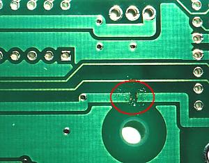 |  |
There is a pattern of +5V in a power circuit. It may short-circuit, when a stud is attached. Therefore, +5V pattern to a power circuit was cut.
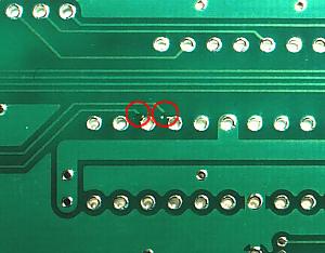
The portion which cut the pattern should apply flux, in order to prevent corrosion. | The signal lines are connected to the RS232C circuit from PIC. Since IC(U5) for RS232C was removed, there is n problem. However, the patterns connected to the RS232C circuit were cut for safety. |
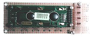
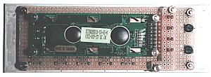
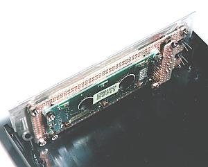
Mounting of parts
 |  |
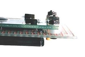
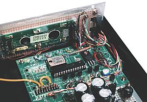
| This is in the state where the parts of a receiving circuit were mounted. There is no modification of this board.The parts which are not used are not mounted. |
 | 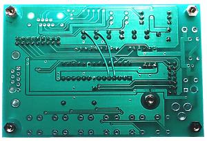 |
| This is in the state where the parts of a display processing circuit were mounted. Several pattern change is made. Some parts, such as parts attached outside, are not mounted. |
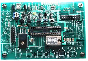
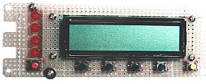
Front Panel assembling
 R9 is a resistor for the LCD backlight light control. A chip type is used. R9 is a resistor for the LCD backlight light control. A chip type is used.
J3 is the switch terminal of the backlight. Since the backlight is always turned on with this equipment, J3 has been short-circuited with solder. The form of J3 terminal is two patterns of a semicircle form. Between patterns is connected with solder.
 |  | Form of J3 |
|
 |
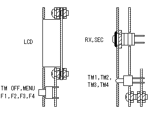
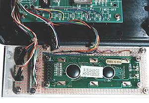
Switches, such as TM OFF and MENU etc, are mounted on the board of the base.
LCD, LEDs, etc. are mounted on a sub board and adjust height. |
| The printed circuit board of the upper photograph is a board for carrying LCD, switches, and LEDs. |
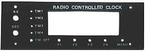
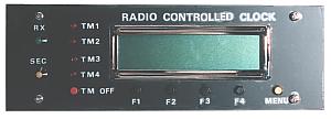
This is in the state where the name was printed on the front panel using the seal. |
 |  |
| Several insulated washers are used for the mounting height control of LCD. |
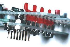
LEDs of TM1, 2, 3, and 4 is carried on a sub board for height adjustment. LEDs are soldered to a sub board in the position to which a tip comes out from a front panel a little.
 |
 |  |
This is in the state where parts were mounted on the board. LEDs of RX and SEC are directly mounted on a front panel.
|
 |  |
This is in the state where parts were mounted on the front panel. |
 |  |
| The cover which prevents the leak of a light is attached in LEDs of TM1, 2, 3, and 4. I made the cover from black paper. | This is in the state which attached the front panel in the case temporarily. |
Making of cable connector
With this equipment, a LAN cable is used as a cable which connects a display processor and a receiver. Therefore, RJ-45 are used for a connector.
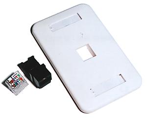 | 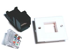 |
| This time, RJ-45 connector suitable for a case was not able to be obtained. Therefore, I decided to process a wall type. | This is the processed connector panel and a connector. |
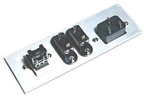
Rear Panel assembling
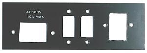 | 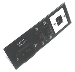 |
| Power connectors ( input, output ) and a LAN cable connector are attached in a rear panel. Since a LAN cable is for connecting a receiver, don't connect it to Ethernet. | This is in the state where the connectors were attached. |
 |  |
| This is the inner side of a rear panel. | This is in the state which attached the rear panel in the case. |
Making of relay fixing bracket
The socket of the relay used this time is the type fixed to the hole made in the board. I created the fixing bracket with the aluminium board of 1mm thickness.
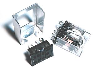 | 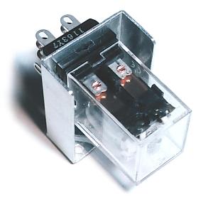 |
| The board of aluminum is bent first. After making a hole, it is difficult to bend. It will no matter, if you have an exclusive tool. | This is in the state which attached the relay in the bracket. |
Wiring
 |
This is in the wiring situation of the front panel.
The length of wiring is giving the margin a little. |
| A position is checked before attaching each unit in a case. |
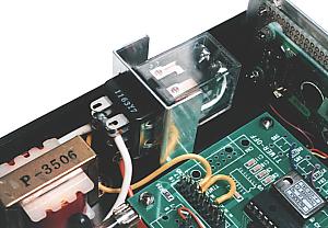 |  |
| This is wiring of a relay circuit. | This is in the state which attached the front panel in the case. |
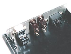
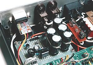 |  |
| This is in the situation of the connector wiring which connects a receiver circuit. | This is wiring of the power supply section. |
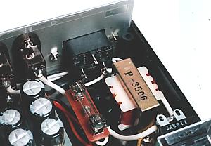
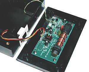 | 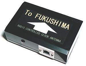 |
| This is wiring of a receiver circuit. They are only the wiring for display processing circuits, and LED wiring for TCO. | I stuck the label showing the direction of a transmitting station on the case of a receiver circuit. |
|