Printed Wiring Boards
|
When assembling an electronic circuit, a board is needed on which the components can be mounted and wired together. This board is called a Printed Wiring Board (PWB). In Japan, the printed wiring board used to be called a "Printed Circuit Board." Nowadays in Japan the name "Printed Circuit Board" is not used because the initials of "Printed Circuit Board" are "PCB." PCB also stands for "Polychlorinated Biphenyls (PCBs)," which is a poison. So in Japan, we refer to the boards as "Printed Wiring Boards." In other countries, they are still refered to as "Printed Circuit Boards," or PCBs. Making a PWB takes a lot of work, and can be very difficult. For this reason, for many hand-made circuits, I often use a universal PWB. The universal PWB consists of an insulation board drilled with .8mm holes at 0.1 inch (2.54 mm) intervals. The board is completely covered with these holes from edge to edge. The insulation board is comprised of fiberglass (glass epoxy), paper epoxy, or bakelite plastic. Centered around each hole on the bottom of the PWB is an (approximately) 2mm copper leaf (known as the "land" or "pad"). To use the board, the parts are mounted on the face of the board, and the component leads are passed through the nearest holes, to project through the bottom of the board, where the wires can be soldered together. The interval between the holes is 0.1 inches (2.54 mm), so DIP or SIP ICs can be easily mounted. 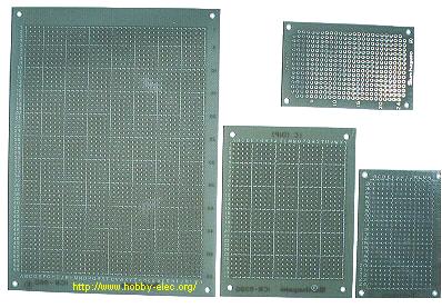 The photograph shows a PWB made of glass epoxy. The color is green. Paper epoxy boards have a beige color. In case of bakelite, the color is thin brown. As for the size of the board, there are several kinds by the number of the holes. From the left side in the photograph 55 x 40 holes (size 160 x 115 mm) 30 x 25 holes (size 95 x 72 mm) 25 x 15 holes (size 72 x 47 mm) There are various sizes in addition to what I have shown, so you can select a board according to your needs. The boards can also be cut to size. On the top right in the photograph, the back side is shown. The copper leaf on this board has been pre-soldered ("tinned") to make soldering easier, so it has a silver color. If the board has not been pre-soldered, then it is seen to have a copper color. |