Image correlation is a useful technique as it allows you to compare current
and previous images and detect which has been moved and in what direction.
In the optical mouse the images in use are successive images of the suface
that the mouse is moving over. By comparing (correlating these) the direction
and speed of the mouse can be determined.
More modern optical mouse designs use a CCD image detector but use the same
principle.
An optical mouse utilizing a linear array of photodiodes is provided with
circuitry to correlate during each self-timed cycle a new image with a stored
image from the previous cycle with the new image offset relative to the stored
image one pixel (photodiode signal) to the right, one pixel to the left,
and also with no offset.
All three correlations are done at the same time in separate correlators.
Decision as to motion to the right, to the left or no motion is made on the
basis of maximum correlation output. The new image is not stored in a second
store array for use during the next cycle until any motion is detected, but
it is stored in a first store array during the cycle when half the precharged
photodiodes discharge below a predetermined level in response to incident
light.
A new cycle is initiated by precharging the photodiodes when any decision
of motion or no motion is made.
This design relates to an optical motion detector of the type commonly referred
to as a "mouse" because the body, which fits easily in the palm of the hand,
is intended to be moved on a desk top with a cable connecting it to a computer
resembling the tail of a mouse. The detected motion of the mouse is used
as an input to the computer for such purposes as positioning a cursor on
an image or text displayed on a cathode ray tube, or as an input to graphics
being generated at the computer console.
The mouse is quickly becoming popular. Older mechanical mouse designs are
being replaced by new designs that use optics instead of moving parts to
detect motion. These optical mice improve the reliability and decrease the
intermittent action so common with mechanical mice.
To date, all the optical mouse designs must be moved over a special surface
pattern in order to sense their motion properly. One commercially available
optical mouse uses a metal plate as a working surface on the desk top with
orthogonal grid lines. Lines in one direction reflect infrared and lines
in the other direction reflect visible light.
Sensors within the mouse that are sensitive to only one color of light can
thus detect motion in two directions independently. R. F. Lyon of Xerox
Corporation developed an innovative optical mouse that integrated sensors
onto the same chip with the processing of optical signals for detection of
motion.
However, his design requires a working surface consisting of a hexagonal
grid of dark dots on a light background. An object of this design is to relax
the requirements on the working surface of the optical mouse. The object
is to make an optical motion detector general enough to allow it to work
on a wide variety of surfaces like those commonly found on desk tops, thus
eliminating the need for a special working surface.
In accordance with the present design, an optical motion detector is comprised
of a single chip having an array of photodiodes and means for focusing an
image onto the chip. The chip also includes an array of storage devices to
store an image, and means for correlating pixels of a current image with
pixels of a previously stored image, means for determining the position where
the correlation is the greatest by correlating the old image in line with
the new image and the old image offset one pixel to the right and again offset
one pixel to the left of the new image, and a self-timed control means to
sequence the operations.
The position of correlation with the old image offset to the right or the
left indicates the relative motion of the image during the interval between
one cycle of storing and correlating an image and the previous cycle. The
self-timing is effective upon the total charge of all photodiodes initially
charged falling below a predetermined level in response to discharge by leakage
current caused by an optical image to assure that the array does not move
more than one pixel width during one cycle.
A circuit connected to receive the outputs of the correlation means allows
each correlation output to inhibit other correlation outputs of lower amplitude
to assure a clear decision of the direction of motion, or a decision of no
motion.
In a preferred embodiment, a second array for storing an image is provided,
and the new image correlated is not transferred from the first store array
to the second until a decision is reached that there has been a movement
to the left or right. However, every decision of left move, right move or
unmoved, is effective to initialize another cycle to receive and store a
new image in the first store for correlation. This arrangement reduces the
rate of movement that can be detected to zero.
The novel features of the design are set forth with particularity in the
appended claims. The design will best be understood from the following
description when read in connection with the accompanying drawings.
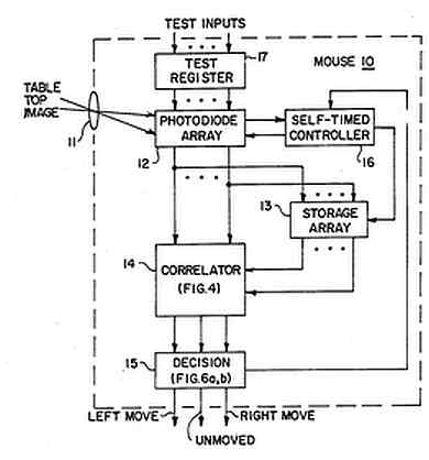
Referring to FIG. 1, the optical motion detector consists of a single nMOS
integrated circuit chip 10 and a lens 11 to project an image onto the chip.
FIG. 1 shows the chip in a functional block diagram form. It consists of
an array of photodiodes 12 for detecting a light pattern image, a storage
array 13 for the image, a correlator 14 to compute the correlation between
the stored image and a current one, decision circuitry 15 to determine the
direction of motion and a self-timed controller 16 to sequence the entire
system.
Also included is a test register 17 that can electrically simulate optical
images, allowing the chip to be tested for fabrication defects in a conventional
nonoptical setting.
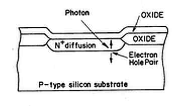
The optical transducers are photodiodes implemented in an nMOS integrated
circuit chip. In this nMOS chip, a region of N+ diffusion forms
a diode with a grounded p-type substrate, as shown in FIG. 2a in a cross
section. FIG. 2b represents the photodiode by a reverse biased diode
D1 having a capacitor C in parallel.
Photons striking the circuit side of the chip forms electron-hole pairs that
create a leakage photocurrent through the reverse biased diode. In operation,
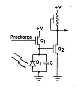
the diodes of the array are each precharged by a separate enhancement mode
FET pull-up switch Q1 which then shuts off leaving them
isolated.
The diodes then discharge due to the photocurrent at a rate proportional
to the intensity of the light striking the diffusion region. Thus for imaging,
an array of these photodiodes starts out with all diodes charged. Each photodiode
discharges at a rate determined by the intensity of the image at that
point.
Eventually all diodes are discharged. Associated with each photodiode is
a pull-down FET switch Q2, the function of which will now be described
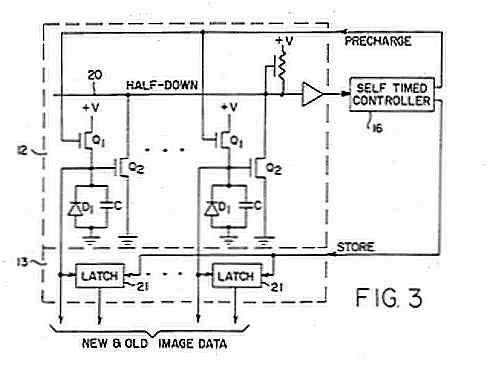
with reference to FIG. 3.
Charge patterns that reflect interesting properties of the image occur somewhere
between the time when all the photodetectors are high and when all of them
are low. In this exemplary embodiment of the design, all photodiodes are
sampled and stored at once, at a time when half of them are below a threshold
and half of them are above.
This approach maximizes the information content in each pixel. The circuitry
to accomplish this operation is shown in FIG. 3. There is a global half-down
line 20 with a single pull-down FET switch Q2 for each photodiode.
When the diodes are all charged high, the pull-down FET switches
Q2 are all on.
The half-down line is low, with each of the diodes contributing to the pull-down
current. As each photodiode discharges and passes the threshold of its pull-down
FET switch Q2, the FET switch Q2 turns off, subtracting
its current from the total pull-down current. When the total current decreases
far enough, the half-down lines goes high.
This threshold is chosen by the width/length ratio of pull-up and pull-down
FET switches to occur when about half of the photodiodes are down. The rise
of the half-down line triggers the self-timed controller 16 which in turn
triggers latches 21 of the storage array 13 to end their sampling of the
falling photodiode values.
Positive feedback in each of the latches turns the stored signal into a restored
digital signal for each pixel. The digital image in these latches, one bit
per photodiode, is later compared with the next image.
Given two consecutive time samples of an image, the task of motion detection
becomes a comparison of the two images. Under the assumption that the object
in view has changed relatively little, the images should be nearly the same
except for a translation that corresponds to the motion. One method of detecting
that motion is to shift one image past the other in both directions, and
at each position of the shift, sum the number of bits that match.
The position where this sum is the greatest will indicate the direction the
image has moved between samples. How much it has moved is a function of the
time between samples and the velocity of the mouse. The extent of motion
must not exceed the space between diodes for each sample-and-compare cycle.
This comparison and summing process corresponds to a one-dimensional correlation
function. The continuous version is given by the formula:
I0 is the image at time=0, and I1 is the next image
sample taken at time=1. The correlation of I0 and I1
is C(s), where s is the amount one image is shifted relative to the other.
The discrete approximation to the correlation function is given by:
If the motion detector can operate fast enough to guarantee that the fastest
motion never moves the image more than one photodiode (pixel) width between
two consecutive time samples, then this computation need only be performed
within a one pixel neighborhood. The number of correlation values to compute
and compare is then only three for the one-dimensional case: C(s) where s=-1,
0 and 1. These values correspond to the image having moved left by one pixel,
not having moved, or moved right by one pixel.
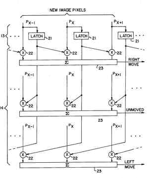
The logic diagrams for the correlators are shown in FIG. 4. Each of the three
required correlation values are calculated by performing a multiplication
of each of the old image pixel values with the corresponding new image pixel
values in one bit multipliers 22 and summing the results in a circuit 23.
The only difference between the three correlators is the amount the old image
pixels are shifted relative to the new image pixels.
When the analog voltages on the light sensors (photodiodes) were stored,
much of the light level information was lost. This information was sacrificed
for the ability to have long term storage of the image. In the correlation,
two consecutive images could be digitized and the correlation performed on
them.
Instead the present design retains as much of the analog information as possible
and utilizes it in the correlation computation. The correlation is performed
between pixels of the previous image, stored as 1-bit digital values, and
pixels of the current image which are analog and develop in time from an
all high state toward an all low state.
The correlation values are thus analog voltages that develop during the cycle
as the photodiodes discharge.
Exclusive NOR gates could be used to do the multiplications in the correlation
computation. For this case, the individual correlation values within a cycle
start out at an intermediate value when the photodiodes are all high, rise
to a peak in the middle of the cycle and return to an intermediate value
when all the diodes are discharged.
To determine which correlation was the greatest would require first finding
the peak voltages of each time-varying correlation output and then comparing
them. Determining when all the peaks have passed so that the self-timed cycle
can start over is a difficult analog circuit problem, especially when the
circuits must work with continually changing light on the photodiodes, and
must work over several orders of magnitude of speed range.
There is a better way, using AND gates to perform the multiplications.
Correlation values using AND multiplication are monotonic as they develop
in time from an intermediate value when the photodiodes are all charged to
a zero value when the photodiodes are all low. This monotonicity allows the
comparison circuitry to be much simpler.
Now comparing the correlation values is just seeing which of them goes to
zero first. The end of the cycle is much easier to find also. The cycle ends
when the first correlation value goes to zero. Circuits to detect this final
zero condition are much simpler than circuits to detect the passage of a
peak.
It is interesting to note that for motion detection either XNOR gates or
AND gates can be used to achieve the same results. The XNOR function is
equivalent to multiplication for digital levels assigned the values of 1
and -1, while AND gates perform multiplication for values of 0 and 1. The
difference between these two ranges is the simple transformation:
Substituting this transformation into the correlation equation and simplifying
yields the result:
CXNOR (x)=4CAND (x)+constant
This result shows that for the correlation computation, the difference between
using XNOR and AND gates is a simple scaling and translation of the resulting
values. Of importance here are the correlation values relative to each other,
so either type of multiplier will do just as well. It may seem that the XNOR
gate has a built in gain factor of 4 over the AND gate, but in practice,
circuit implementation with either gate would scale the results into the
same range, an analog voltage between the power and ground supply rails.
For simplicity, it is preferred to implement the multiplications using AND
gates.
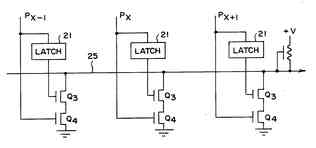
The circuitry to perform one of the three correlations (the unmoved correlation)
is shown in FIG. 5. It consists of a pair of series pull-down FET switches
Q3 and Q4 for each pixel that performs the AND function
required for the 1 bit multiplication by sinking current when both the old
image input and the new image input are high. A global correlation line 25
connecting the pull-down switches performs the current summing function
represented by block 23 in FIG. 4.
For the one-dimensional motion detector, there are three correlation lines,
as shown in FIG. 4. On one of these lines, the current level indicates the
strength of the correlation on the image "moved right" by one pixel. Another
indicates the strength of the correlation on the image "unmoved" and the
last indicates the strength of the correlation on the image "moved left"
one pixel.
This three-way correlation is easily implemented by connecting the new and
the old pixel output terminals so that the old image is effectively shifted
one pixel to the right, not shifted, and shifted one pixel to the left relative
to the new image. The currents on these three lines must be compared to determine
which of the three possibilities has occurred.
The right move, left move and unmoved correlation lines start at a high current,
low voltage state and evolve toward a low current, high voltage state. The
voltage state of the line with the greatest correlation will go high before
the other two. The ultimate comparison for determining motion is made on
this line voltage condition. The comparison is done using mutual
inhibition.
Each of the three correlation lines has a rising voltage that is in a race
with the other two. The winner of the race is the one to reach a high first.
As each line goes high, it inhibits the rise of the other two, pulling them
back down. In this way, the final high voltage line is never ambiguous because
the only possible final state of the system is with one line all the way
high (the winner) and the other two low (being fully inhibited by the
winner).
If two or more lines are rising at nearly the same rate, the time required
for a winner to be chosen is unbounded. The circuit is then in a metastable
condition. In that sense, the mutual inhibition circuit may be viewed as
a 3-way arbiter.
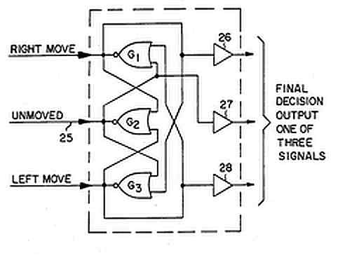
Referring to FIG. 6a, mutual inhibition is implemented by gates
G1, G2 G3 cross-coupled to form a three-way
NOR flip-flop that starts out in the balanced or "illegal" state of all low.
As the three lines are allowed to rise by the correlation circuitry, one
of them will rise high enough to begin pulling down the other two.
The final state of the circuit will be two lines low and one line high indicating
which direction the image has moved (or not moved). When this circuit, identified
in FIG. 1 by a block 15 labeled DECISION, falls into one of these stable
states, it has "decided" which of the three correlation values was
greatest.
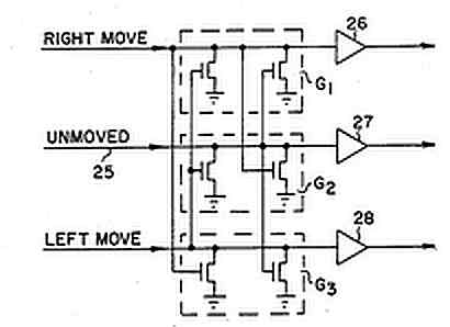
FIG. 6b shows how the decision circuit may be implemented with six FET
transistors in an nMOS integrated circuit.
The buffers 26, 27, 28 driven by the three correlation lines must have high
enough thresholds so that they are not falsely triggered by the lines rising
to their metastable levels. The cross coupling of the gates guarantees that
at most one line will rise past the metastable voltage all the way up.
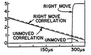
FIGS. 7a and 7b show two plots from simulation of the decision three-way
flip-flop. In the first (FIG. 7a) the correlation value for the right move
is 1.0% higher than that of the unmoved line and the left move line. Here
the right line has no trouble winning the race and going all the way high.
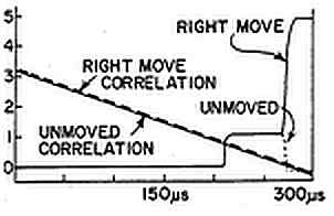
In the second (FIG. 7b), the correlations are only 0.05% different. Here
both lines rise to the point that their mutual inhibition prevents them from
rising further. The simulation shows that they hang for more than 50
μsec near the metastable point before finally one (right move) wins
and goes all the way high.
(These simulations do not take into account thermal noise or on chip device
parameter variations).
The three outputs of the decision circuitry 15 (FIG. 1) buffered by amplifiers
26, 27 and 28 are outputs of the chip. They indicate detected movement by
pulsing high from the time the decision is made until the next cycle is begun.
These signals can be further encoded on chip for other motion encoding
schemes.
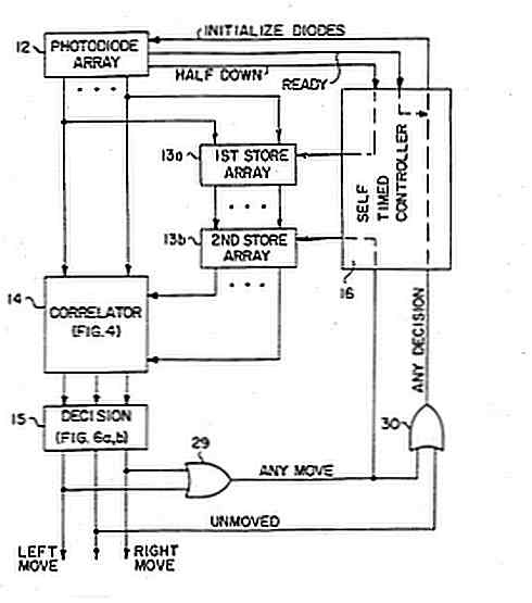
During a cycle there are two independent processes going on. The stored image
from the last cycle is being used during the correlation-comparison process,
and the current image is being stored for use in the next cycle. Since there
is no guarantee that the computation-decision process will finish with the
last image before the current image needs to be stored, there must be a two-level
store, as shown in FIG. 8.
A first store array 13a samples the photodiodes and brings each to a digital
level when half-down line 20 reaches a predetermined level. A second store
array 13b holds the previous image samples for the correlation computation.
The image is transferred from the first store to the second in response to
any move made by the decision circuitry via an OR gate 29.
If the image moves by less than half a pixel between samples, the greatest
correlation will always be on the unmoved line. If the second store 13b always
contains the previous sample, continuous motion at speeds less than half
a pixel per sample will never indicate a motion. For each cycle, the best
image match will always be for the unmoved position.
This occurrence is clearly a problem since the maximum speed of the image
is only 1.5 pixels per sample (for a motion detector that only calculates
correlation in a 1 pixel neighborhood). A good motion detector should have
no minimum velocity, especially not one so close to its maximum velocity.
This problem is solved by keeping the old image in the second store 13b if
an unmoved condition occurs. The only time the new image is moved into the
second store used for comparison with successive images is after a movement
is detected, as shown in FIG. 8, using the OR gate 29 to trigger the second
store if any movement is detected.
This technique reduces the minimum velocity of the motion detector to zero.
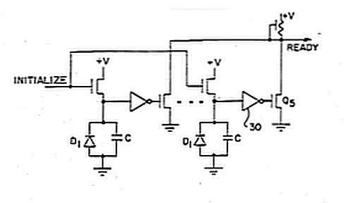
Since the cycle is self-timed, some circuitry is needed to detect when the
photodiodes have all reached their high precharged level. FIG. 9 shows how
a distributed NOR gate comprised of FET switches Q5 coupled to
the photodiodes D1 by high threshold inverters 30 are used to
generate the required ready signal. If any of the diodes are below the threshold,
the ready line will be low. When all photodiodes are pulled high enough,
the ready line goes high.
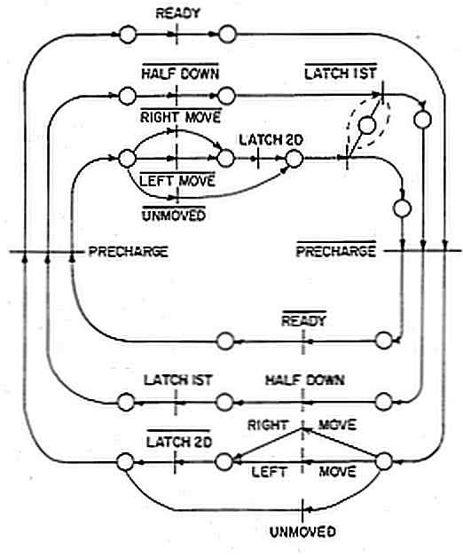
A Petri net of the flow of events in the motion detector is shown in FIG.
10. Note that the half-down and ready transitions are not truly independent.
The ready line always goes low before the half-down and goes high after the
half-down condition. There is an extra pathway, shown by dotted lines, that
serves to synchronize the first and second latches.
This link guarantees that the image data is transferred to the second store
array 13b before the first store array 13a is cleared in preparation for
the next cycle.
It should be noted that the self-timed controller 16 shown in FIG. 8 is
represented schematically as simply a "junction box" between controller inputs
and outputs, but that in pratice the self-timed controller implements the
functions necessary in accordance with the Petri net shown in FIG. 10.
Basically, any move triggers the second store array 13b, and any decision
of motion or no motion initializes the photodiode array 12. Following that
the ready signal generated in the photodiode array 12 as shown in FIG. 9
will terminate the initializing (upper) part of an imaging cycle shown in
FIG. 10.
Thereafter, the half-down signal triggers the first store array 13a, indicated
as LATCH 1ST in FIG. 10. The primary selftimed controller function is just
that simple, but may in practice be more complex in order to take circuit
details into consideration as has been done in the Petri net of FIG. 10.
When the photodiodes have been precharged, the ready signal generated will
indicate to the self-timed controller that the photodiodes are fully charged
so that the imaging part of a cycle may commence, which is the lower half
of the Petri net in FIG. 10. The ready signal thus effectively stops the
initializing of the photodiodes.
When the imaging part of the cycle is done, the output of OR gate 30 again
initializes (precharges) the photodiode array. Meantime, if there has been
any move, the output of the OR gate 29 transfers the content of the first
store array 13a to the second store array 13b.
A one-dimensional motion detector chip was designed and fabricated using
a single poly, single metal nMOS process with buried contacts and 4 μm
minimum device size (λ=2 μm). The chip was 5711.times.1734
μm and contained sixteen photodiodes in a linear array. Each photosensor
was a diffusion rectangle 200.times.400 μm. The chips came packaged
in 40 pin packages with cavity covers that could easily be removed to project
images onto the chip.
The operating frequency of the optical chip is a function of light level
because the discharge rate of the photodiodes is the major delay in the cycle
of operation and that rate is proportional to the intensity of the incident
light. The operating frequency, f, is given by the equation:
where t is the time for one cycle, L is the illuminance of the incident light
and k is a constant. Experimental results show that this liner approximation
is reasonable over almost three orders of magnitude of light level variation.
The theoretical proportionality constant for the frequency/light level relation,
k, can be calculated from the unit area capacitance of the diffusion layer
and from a conversion between incident light and photocurrent.
Depending on the exact assumptions made, k is easily within a factor of 2
of the experimental results. For the chip that was built, a first order
approximation shows that frequency varies linearly from about 5 kHz to about
500 kHz for the intensity of light of a flashlight at 3 inches at one extreme
and sunlight at the other (lumen/meter2 of flashlight about 50
and of sunlight about 5,000).
This range of frequencies will yield a maximum motion tracking speed of about
1 meter per second at one extreme to 100 meters per second at the other
extreme.
If the image moves on the chip between image samples farther than the
neighborhood of correlation calculation, the motion detector will not accurately
report the motion, since the correlation is calculated only to the nearest
neighbor, about the width of one diode or about 200 μm. At room light
levels, the free running cycle frequency of 10 kHz corresponds to an image
velocity of about 2.0 meters/second.
The magnification provided by the lens is the ratio of the size of the image
on the chip surface to real object. In a mouse application, a magnification
of 1 gives a resolution of about 100 points/inch and a maximum mouse speed
of 2.0 meters/second.
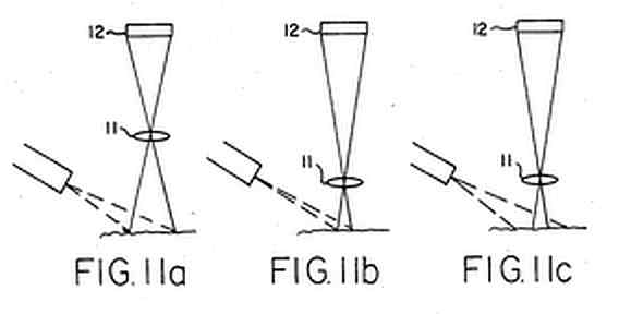
The magnification can be changed by moving the positions of the lens and
chip relative to the object. Adjusting the magnification effectively trades
off resolution for maximum tracking speed. See FIGS. 11a, 11b and 11c. In
FIG. 11a the lens is positioned to image a large illuminated area for high
maximum speed, but low resolution.
If the lens is positioned closer to the object for imaging a smaller area,
as shown in FIG. 11b, and all of the light from the illuminator is concentrated
on the imaged area, a high resolution will be achieved, but with a low maximum
speed. Should the light from the illuminator cover more area than is being
imaged, as shown in FIG. 11c, i.e., if the intensity of the light on the
imaged area is reduced, high resolution will be retained, but the maximum
speed that the mouse can track is even lower than for the arrangement of
FIG. 11b.
Thus it may be appreciated that by correlating the present image from a linear
array of photodiodes with the previous image (1) shifted to the right one
pixel, (2) not shifted, and (3) shifted to the left one pixel during each
self-timing cycle, any motion in either direction of the linear array may
be detected.
To additionally detect motion in any other direction, such as normal to the
linear array just considered, a second array normal to the first may be
incorporated together with its complete and independent circuits.
See also:
| file: /Techref/io/opticalmouses.htm, 33KB, , updated: 2015/12/20 16:08, local time: 2025/10/20 14:13,
216.73.216.53,10-2-207-162:LOG IN
|
| ©2025 These pages are served without commercial sponsorship. (No popup ads, etc...).Bandwidth abuse increases hosting cost forcing sponsorship or shutdown. This server aggressively defends against automated copying for any reason including offline viewing, duplication, etc... Please respect this requirement and DO NOT RIP THIS SITE. Questions? <A HREF="http://www.massmind.org/techref/io/opticalmouses.htm"> Optical Mice IO</A> |
| Did you find what you needed? |
Welcome to massmind.org! |
|
The Backwoods Guide to Computer Lingo |
.