Ok. We have had our fun. Surely designing the circuits is MUCH more fun than making them work. Making them work can only be described as work, but its' necessary to get something we can lay our hands on. Besides, just doing paper designs isn't very fulfilling after awhile. There's just no getting around it, we have to make it work. How tough can that be?
Well, for static rams, not too bad. But, for dynamic rams, it can be tough. When a dynamic memory device cycles it draws varying amounts of power. Over very short periods of time the demands of a dynamic ram can be severe. the following illustration will introduce us to the power needs of a typical dynamic ram device. The specific device we will be looking at is the Hitachi 4864 used in two of our earlier designs.
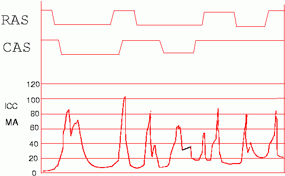
Figure 25 shows the current requirements typical of a dynamic memory chip. In this case, a 64K by 1 device. Note that the most extreme power consumption demand is at the edges of RAS and CAS. It is here that the device is cycling. These current demands are shown to exceed 100ma at times, over periods greater than 50ns.
We need to prepare for two things; the need to provide power during these times, and the effect that these current spikes can have on the memory devices and their drivers. Fortunately these problems are not new. Answers were developed a long time ago that are still valid today. We can treat them as "cookbook" answers, and move on.
The current demands can be met by adding capacitors near each DRAM device. There should be a .1-.33 uf cap across every dynamic memory in the design. When you are using SIMM, you can forget this. There are already capacitors under the DRAM chips on the SIMM PCB. You can't do any better than this, so don't try.
For designs like our first three, you should locate a bypass capacitor physically near each memory device. The traces connecting the capacitors to the memory devices should go directly to the power pins of the DRAM chip, and be as heavy as possible; fifty thousandths at LEAST. It is these capacitors that will provide the instantaneous current that the circuit demands. If you are hand wiring your circuit, lay the capacitor across the package and solder the leads directly to the power pins of the memory chip. Remember. One for each chip. Don't skip any.
For older technology DRAMS, up to 64K, you should use .1uf capacitors. From 256K and up, you should use .33uf. These devices require even more current than their predessors. In addition to the bypass capacitors you should provide solid tantalum capacitors located near the memory array. These tantalum capacitors should be 4.7uf to 10uf. For a small memory array I would prefer 10uf. For a large array I would prefer 4.7uf. This would spread the capacitance around the array.
The .1uf, or .33uf, capacitors will provide the current needed by the DRAMs when they are cycling but they need to be recharged between current spikes. The solid tantalum electrolytics will do this. You may use either the axial lead rolled tantalum capacitors, or the dipped tantalum capacitors.
How many electrolytic capacitors you will need is a function of how many DRAM devices you are going to use, and the construction techniques being used. If you are using a multi-layer board, use one tantalum capacitor per row of memories, or per SIMM socket.
For the rest of us, we will need more. For a two layer board, or a hand wired board, use one tantalum capacitor at each end of every row of memory chips.
Keep this in mind. There is no power supply made that can supply dynamic memories what they need. The capacitors in the power supply are too large. They wouldn't be able to respond in time to smooth the spikes. Also, the regulators in your power supplies can't respond fast enough. They operate in millisecond time frames. The current spikes generated by our DRAMs would be totally invisible to the main power supply.
The second thing we said we had to deal with is the effect that these current spikes can have on the memory devices, and their drivers. Follow me through an example. In examples two and three we used the 4864 64K DRAM device. There were eight of them. If we take the worst case current demands from figure 25, 100ma, and multiply by eight devices we get 800ma of current. That is nearly an ampere of current needed in the span of 50ns of time.
What is the resistance of the etch you used to connect the power supplies to the memory array, and their drivers; .1 ohm, .2 ohm? From Ohm's law we compute the voltage drop across that etch 0 (during the power spike; E=I*R. If current is .8 amperes, and resistance is .1, or .2, ohms, then we calculate that voltage is .08, or .16, volts.
If the wire we are discussing is the ground connection to the memories we have a problem. If the etch resistance is .1 ohms the ground potential of the memories will RISE by 80mv. If the resistance is .2 ohms, the ground potential will rise by a whopping .16 volts. That is almost the zero level detection voltage of a TTL compatible device.
I know. You are going to tell ma that a legal logic zero is .8 volts or less. I know this, but it seems that many new CMOS parts don't. They want .2 volts for a logic zero. Ok. Here's what we have. If the ground potential of the memories is raised by .16 volts with respect to the memory drivers, then it may be impossible for the memory to drive the data bus low enough to register a logic zero at the Z80's data pin. Result? It doesn't work, and you can't figure out why. You wired it exactly the way I told you to. You can even do a continuity check of the circuit with an ohm meter, and its' right. But, it still doesn't work. Now we're getting to the meat of the issue.
This is the kind of stuff that gray hair is made of. It is this kind of problem that has caused some to think that DRAMs take black magic to make them work. I have seen many prototypes built with DRAMs that didn't work, and should have. OK. How do we make them work? Don't hold out on us now!
The first, and most important, thing is to use adequate trace widths to feed power to the dynamic memory array. How do you know what is enough? Some times the only way would be to build it and see if it works. This isn't practical, so we will design in a lot of overkill, or gaurdband. Use the heaviest power traces you can to feed the memory array. When locating the parts on your PCB, try to locate the memories as close as possible to the source of power. If possible, run the power feed to the memories FIRST, then to the drivers. Consider the following illustration.
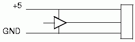
In figure 26 above we see a possible power feed for one of our designs. Notice that both +5 volts, and ground, are physically connected to the driver before they are connected to the memory array. The trace between the driver and the memory array now must supply all of the current required by the memory. The resistance of the trace between the driver and the memory array is the what we are examining. When the memories cycle, this trace must supply the current demand. When the memories cycle, both the +5 volts, and the ground potentials of the memory array will be shifting. This is not a good way to wire a dynamic memory array. Let's look at how to do it right.
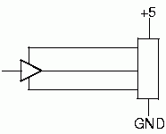
In figure 27 above we see the correct way to route power to our memory array. The power connections are made directly to the memory array with as wide, and short, a trace as possible. The power connections to the driver chips, in our case the 74157's, are made with as short a trace as possible from the memory array to the driver chips.
Now we have a design that will probably work. When the DRAMs demand their switching current, we have the bases covered. We have the .1uf to .33uf caps right at the memory chip, and we have the tantalum electrolytic at the end of each row of chips. We have a good solid power feed to the memory array, and a good feed from the memory array to the driver chips.
When the current spikes occur, we can supply the current needed by the memories. If the ground potential does shift, it will be with respect to the power supply pins, not the drivers. In fact, the traces connecting power to the drivers now only have to feed the drivers. This is much easier than feeding the whole memory array. Further, the 74157's don't have the extreme power needs that the memory chips have. There will be very little voltage drop across those traces. If the ground pin of the memory does shift, with respect to the power supply, the drivers will shift with it. Thus, there is no problem with detecting logic thresholds on the DRAM inputs.
We also separate the power feed to the rest of the board. If necessary, feed the Z80 from the power pins of the memory drivers. If everything maintains the same ground potential, we have largely whipped our problem. The feed for the +5 volts is important too, but ground is more important.
OK. that's all fine and good if we're ready to lay out a circuit board. What if we want to hand wire the board. Beware! Shark infested waters are close at hand. Hand wiring dynamic rams requires special care. But, it CAN be done.
It doesn't really matter whether you are using a wire wrap gun, or you are hand wiring using point to point techniques. The solution is the same; put your wire wrap wire away. The wire used in wire wrapping will not work for power connections. It is usually either #30, or #28, wire. This wire is O.K. for no more than about 30ma of current. Any more than that and you need to review our discussion about the resistance of the wire. Use #12 solid copper wire. You can get it pre-tinned by the roll, or you can use a piece of house wire. that's right. A piece of #12 ROMEX will provide all the wire you need. Strip it of all insulation and keep the bare wire. A length of #12 copper wire in free air can conduct approximately 30 amperes. This will give us a very low impedance power bus.
I prefer the kind of prototype boards that have a pad per hole. You can use this to anchor the #12 wire to. I will flow solder down the entire length of the wire. First, determine what type of power connection you will make to the PCB. If you are going to plug it into a bus structure, like the PC ISA bus, make the connection directly to the edge connector finger. Don't worry that the edge connector finger is not as heavy as the wire I'm making you use. The actual equation for the resistance of the wire is the sum of a series of resistances. Also, use every power pin on the connector; ground too.
Bend the wire to form it to how you want it to run, and solder it down to the board. Remember. If possible, make the connection to the memory array first, then feed the rest of the board.
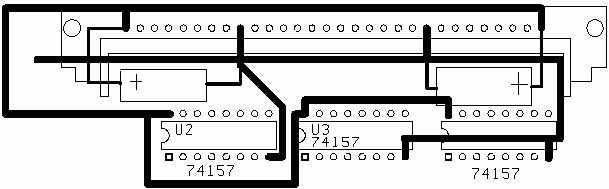
In figure 28 above we see a sample parts placement, and power wiring, for a single 30 pin SIMM socket such as we used in our last design example. The heavy black lines are the #12 solid copper wire. Observe how the ground wire connects to the memory array (the SIMM socket in this case) first, then goes to the drivers. The power feed to the circuit is on the left. The wire hanging loose is the ground wire. This is the point where it enters the board. The wire to its' left, that seems to be forming a "U" is the +5 volt feed. It was not possible to feed +5 from the SIMM socket directly to the driver chips as all of these wires are on the bottom side of the board, and they are uninsulated. However, the +5 volt feed is not as critical as the ground feed.
This arrangement will work well. Also, note the electrolytic capacitors connected directly to the SIMM power pins. These are our solid tantalum electrolytics. I prefer 10uf capacitors.
The solid copper #12 wire should also be used to route power to as much of the board as possible. If it is not possible to reach every chip with the #12 wire you can solder a wire wrap post to the #12 copper wire by inserting it into a hole adjacent to the solid copper wire, then forming a solder bridge to make the connection. You can then wire wrap to this post. Use only #28, or heavier, wire to make connections to I.C.'s, and make the wire as short as possible. I will frequently use two #28 wires per power pin of an I.C.
There is another consideration that can effect the success, or failure, of any project that uses) dynamic memories. Such projects also typically include octal buffer/driver devices such as 74xx244, 74xx245, etc. These devices are great at driving busses, but draw a lot of power when switching.
When an output switches state it draws power. A current waveform of a 74LS244/245 would look very similar to figure 25 except that it is a little more complicated. When a 244/245 output is driving a bus line the amount of current that it draws is a function of how many outputs change state at the same time. This is called SSO, or Simultaneously Switching Outputs. The worst case would be for all the outputs to switch at the same time. Most 244/245 devices can drive 24ma per output. This is great when you need to drive a backplane, but watch out for the total current. If you are driving 24ma, and all 8 outputs switch at the same time, we are talking about .192 amperes. Multiply this by how many of these devices you have on the board and it will become very clear what you are dealing with. 74LS244/245's are seldom used alone. They love company. When you see one, you'll see several of them. These devices should be treated to the #12 solid copper feed wire just like your DRAM array. Use the wire wrap post for smaller devices, such as 74LS00's.
When building the circuit in example number five, I spent a day and a half working out the power wiring using #12 solid copper wire. When I got around to wiring the netlist, it took me three hours. The DRAM design worked first try. This should give you some idea of the relative importance of the power routing and wiring.