By placing two PN junctions together we can create a bipolar transistor. In a PNP transistor the majority charge carriers are holes and germanium is favoured for these devices. Silicon is best for NPN transistors where the majority charge carriers are electrons.
The thin and lightly doped central region is known as the base (B) and has majority charge carriers of opposite polarity to those in the surrounding material. The two outer regions are known as the emitter (E) and the collector (C). Under the proper operating conditions the emitter will emit or inject majority charge carriers into the base region, and because the base is very thin, most will ultimately reach the collector. The emitter is highly doped to reduce resistance. The collector is lightly doped to reduce the junction capacitance of the collector-base junction.
The schematic circuit symbols for bipolar transistors are shown in
figure 5.1.
The arrows on the schematic symbols indicate the direction of both
![]() and
and ![]() .
The collector is usually at a higher voltage than the emitter.
The emitter-base junction is forward biased while the collector-base
junction is reversed biased.
.
The collector is usually at a higher voltage than the emitter.
The emitter-base junction is forward biased while the collector-base
junction is reversed biased.
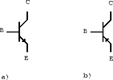
Figure 5.1: a) NPN bipolar transistor and b) PNP
bipolar transistor.