Bipolar junction transistors have low input impedance, small
high-frequency gain and are non-linear when ![]() V.
The input impedance is naturally restricted by the forward-biased
base-emitter junction.
There are always problems due to the main charge carriers passing
through the region where the majority carriers are of opposite
polarity.
V.
The input impedance is naturally restricted by the forward-biased
base-emitter junction.
There are always problems due to the main charge carriers passing
through the region where the majority carriers are of opposite
polarity.
The junction field effect transistor (JFET) overcomes some of the problems of the bipolar junction transistor. JFETs come in two types: N-channel and P-channel, and are shown in figure 5.14.
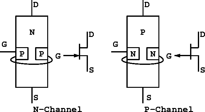
Figure 5.14: Basic geometry and circuit symbols of JFETS.
The designation refers to the polarity of the majority charge carriers in the bar of semiconductor that connects the drain terminal D to the source terminal S. Since the channel is formed from a single-polarity (unipolar) material, its resistance is a function only of the geometry of the conducting volume and the conductivity of the material. The JFET operates with all PN junctions reverse-biased so as to obtain a high input impedance into the gate.